What Are Differential Pairs and Differential Signals?

Differential pairs provide a novel way to route high data rate bitstreams, where each edge transition generally has a very fast rise time. Differential protocols used in high-speed designs are the mainstay of many common signaling standards with familiar acronyms. USB, HDMI, Ethernet, and many more are all routed as differential pairs and will require careful trace design and routing. In the past, this require making many manual corrections to the lengths of differential pairs to ensure they met length objectives and impedance tolerances. However, newer CAD software makes it easy to encode these requirements as design rules to ensure accurate routing.
In this article, we’ll provide a basic overview of the behavior of differential signals and the function of differential pairs. These signal types are standard in high-speed signaling protocols, but they might appear in simpler devices, so it is important to understand how these are routed in a PCB layout. We’ll also provide some more specific definitions of differential pair routing impedance and how noise functions in a differential pair, and hopefully new designers can get a better idea of the importance of differential protocols.
The Basics of Differential Signaling
Differential pairs are very simple: they are composed of two traces, routed side-by-side, and that carry equal magnitude and opposite polarity signals on each trace. In high-speed digital protocols, data is sent over single-ended traces in a PCB that is impedance controlled; each individual trace is designed to have a specific impedance. This is done using a standard impedance-controlled trace design approach, where the width required to reach a target trace impedance is determined after the stack-up is designed and the layer for routing differential pairs is selected.
Differential signaling is not necessarily made up of special types of signals. All differential pairs used to carry digital data will still carry binary information, or possibly multiple bits at once with a more advanced protocol like PAM4. The difference between a standard digital trace and differential signaling is that a differential signal is recovered and interpreted in a different manner.
If we look at the signal propagating on a differential pair, we really have two signals with opposite polarity, but the same magnitude. The signal level that is read by a differential line receiver is just the difference between the voltages of the two signals. This is shown in the figure below.

In the above image, we have a differential pair being routed over a uniform ground plane. These are assumed to be routed on a surface layer as impedance-controlled microstrips, although the exact same ideas apply to strip lines on an internal layer. A component that operates with differential signaling requires that the difference between these two signals be used to interpret a logic level in the differential line receivers. Note that the individual signal levels (V1 and V2) are still defined with respect to the GND reference, which is generally placed as a plane below the traces. In other words, you could measure the signal with respect to the ground on each side of the pair with an oscilloscope if you really wanted to.
This method of transferring digital data (as a pair of opposite-polarity signals on a pair of traces) is standard in high-speed protocols like USB, Ethernet, DDR clock and data lines, and some proprietary digital signaling standards. So what is it that has made differential pairs and differential signaling so successful, and what are some of the challenges? Some of the important advantages and disadvantages are summarized in the table below:
|
|
|
|
|
|
|
|
|
|
|
|
|
|
|
|
Let’s look at these various advantages and disadvantages of a PCB and how they manifest themselves in routing and layout.
Common-Mode Noise Suppression
The ability to suppress common-mode noise without requiring any filtering is unique to differential pairs. Common-mode noise suppression results from the fact that the difference between the two signals is being measured on a differential pair, which can cancel out any noise on differential pairs under certain conditions.
The image below shows schematically how common-mode noise suppression is achieved in a differential pair. If the noise is input into the receiver within the appropriate skew allowance, then it can be canceled by the receiver.

The caveat to this is that the same level of noise must be received on each side of the pair. This could happen on a differential pair that is routed through free space over a cable, so it is not an impossible occurrence. However, this does not mean that differential pairs are immune to crosstalk on a PCB. If you have, for example, a single-ended trace near a differential pair routing, it can couple a crosstalk pulse into both pairs via the magnetic field generated during switching. However, the crosstalk pulse will not be received equally by both traces in the pair; the magnetic field strength. The result is that the noise will not be canceled at the receiver, and some noise may remain on one side of the pair. Make sure that appropriate spacing is applied between single-ended traces and differential pairs to prevent excessive noise from being received on each side of the pair.
EMI Emitted From Differential Pairs
One of the great advantages of differential signals is that they emit low noise. When the two traces in the pair are closer together, the magnetic fields they generate during switching are equal and opposite. As long as the two signals are in-phase and of the same magnitude, the magnetic fields they generate will counteract each other. Note that the generated field is not zero everywhere; this is only true along the centerline between the pair. However, the field will be low and will induce less noise in nearby single-ended traces.
This is another reason differential pairs are preferable for high data rate channels. Serial protocols operating at high data rates (Gbps and higher) will have very fast edge transitions on each bit. Therefore, each trace in the pair will emit strong EMI via the magnetic field during these fast edge transitions (high dI/dt events). With these fast edge rate signals, parasitic capacitance with respect to nearby conductors can be problematic as well as the signal bandwidth might span into high GHz frequencies.

Although differential pairs might produce lower crosstalk in a nearby single-ended signal, they can produce differential-mode crosstalk in a nearby differential pair routing. This is where it’s important to carefully optimize the spacing between differential pairs. Although differential pairs are relatively immune to common-mode noise, they are not immune to differential-mode noise. Keep this in mind when routing your differential pairs and allow enough spacing between pairs to ensure low noise coupling between them.
Immunity to Ground Offsets
The main reason differential pairs are used in long links that might cross between two boards is their immunity to ground offsets. A ground offset at AC or DC can be thought of as common-mode noise; it is a disturbance in the signal that affects each side of the pair in the same phase and magnitude. Therefore, it can also be eliminated by the differential receiver. When the traveling signal crosses a gap between two different ground regions, there is an impedance discontinuity between the two components. It’s possible that a single-ended signal from the source does not have the same voltage at the load because the ground potentials in each region are different. As a result, the receiver will read out the correct voltage carried by the signal because the differential signal level does not depend on the potential difference between two different GND regions.

If you’ve created your PCB properly to support high-speed components and routing, you should only have a uniform ground potential throughout the design through the use of a uniform ground plane in the design. Although differential signals can withstand a ground offset between different grounds in a PCB, designs that run at high enough frequencies/speeds such that they require differential pairs should be routed over a uniform ground plane in any case.
Designing and Routing Differential Pairs
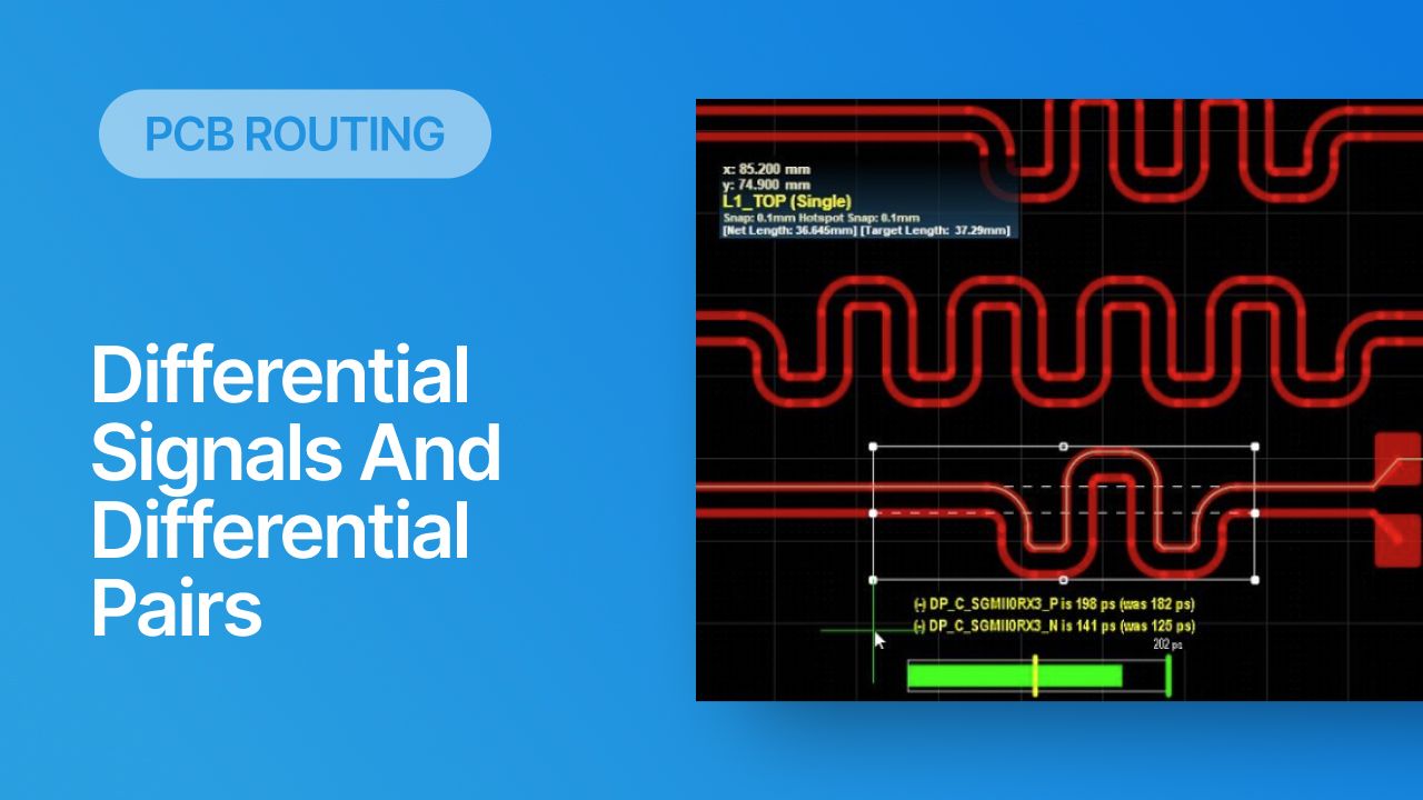
Because differential signals in standard computing protocols and for some peripherals run at high edge rates, they will generally require impedance control to prevent wave reflection off the load end of a differential pair routing. All differential pairs that are used in high-speed PCB design require adjustment of the two sides of the pair to ensure each polarity signal arrives at the receiver at the same time. Here are some of the basic design tips for working with differential pairs:
- Single-ended and differential impedance: Differential signaling standards will specify some single-ended and differential impedance requirements that should be met to prevent reflections and ensure maximum power transfer into the receiver component.
- Delay or length matching: The trace lengths in the pair should be matched within the skew allowance defined within the signaling standard, although this can be rather generous and amounts to several mm for some standards.
- Consistent spacing: My view is that the spacing between the pairs should be set to the minimum value that does not violate impedance constraints. The reason for this is that it will help ensure emitted common-mode EMI is as low as possible and it helps ensure common-mode noise received on a pair as crosstalk has nearly the same magnitude on each trace in the pair.
For high-speed signals, there are other considerations such as signal bandwidth and losses along the link length, which should be considered when selecting materials and components. The best routing tools can help you comply with these requirements by ensuring your design settings are encoded as design rules, and you’ll have automated tools that provide impedance calculations and apply length-matching sections in your PCB.
When you need to design and route differential pairs while ensuring differential signaling integrity, use the complete set of PCB design, layout, and simulation features in Altium Develop. The integrated design rules engine and online simulation tools give you everything you need to verify differential pair routing as you route traces in your PCB. When you’ve finished your design, and you want to release files to your manufacturer, Altium Develop makes it easy to collaborate and share your projects. Experience Altium Develop today!


