


Where Do They All Go? PCB Layout Component Placement Guidelines


When I first learned how to play “Hearts,” I was always worried about how to pass those three cards right off the bat. What if I helped who I was playing against? I got the hang of it eventually and with enough games under my belt. I could recognize card patterns to make the best choices, but until I got to that point it felt like I was throwing random cards across the tables.
My PCB design wasn’t too far off from my card strategy there, in particular with ground plane component placement. I hadn’t learned yet why certain parts had to go next to other parts, nor did I understand that I needed to use the schematic to help me make the best placement decisions. I would base my placement on where the guides were stretching to even if that wasn’t where the part really should go.
Over time though as my PCB design experiences increased my skills, I developed a good workflow for doing my parts placement. There are some important steps during placement such as floor planning and the order in which you place the parts that can be a big help to you if you do them correctly.
Arrange Your Components and Floorplan Your Placement
In the same way that I organize my cards by suits in my hand, I have found that it really helps to arrange all of my parts according to where they need to be placed. I will do this in two steps with the first being floor planning my placement. A floorplan is a sketched-out plan of your parts placement before you start the actual task of putting components on the printed circuit board.
Whether I create this floorplan myself or it comes from someone else, I have found that it’s a good idea to know where all the parts need to go before I start shotgunning components on the screen. This helps me to create a placement that allows for trace routing and even power distribution.
After, I will bring my components onto the screen in logical groups from the schematic. Selecting the components by cross-probing from the schematic is especially helpful for this. I can select a group of components that are all tied together in a circuit, and place that group outside the printed circuit board edge near the location where I know that they will eventually end up based on my floor plan.
Component locations for connectors must be exact to match up with the rest of the system
PCB Layout Component Placement Guidelines
When you are playing hearts you will play certain anchor cards first to strategically accomplish tasks like drawing out the queen of spades. You’ll want to consider your strategy before moving into component placement, too, with some of these PCB component placement guidelines:
-
Place your fixed anchor parts first: These parts will include anything that has to interface with the rest of the system that your circuit board is going to be used in. Connectors, switches, speakers, lights, etc., are all examples of parts that must be placed in fixed locations in order to work with the rest of the system. Mechanical parts such as braces, nuts, bolts, and ejectors will also need to be placed in fixed locations.
-
Place the main component circuitry: Once you’ve got the fixed components in place, you can begin with the main circuitry. Here is where that floorplan will really come in handy to give you a road map of all of your main circuitry.
-
Place bypass caps and other related circuitry: These parts have to be placed in line and next to the components that they are connected to. For instance, resistors that are part of a transmission line can’t be placed clearly over the other side of the circuit board. That would completely ruin the routing topology of the transmission line. Parts like these resistors need to be placed in the same way that the circuit is laid out in the schematic.
-
Be mindful of signal and power routing needs: While it can be easy to get into component placement and forget about the routing needs that separate components require, it is important to keep these in mind to optimize the efficiency of your PCB placement guidelines.
- Check for potential EMI or thermal concerns: Heat, crosstalk, and interference can severely hamper your PCB design capabilities.
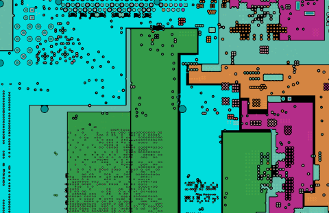
A completely placed circuit board
Finalizing the Placement and Some Tricks that can Help You
Once your fixed components and the main circuitry is placed, you can finish up the placement with the rest of the peripheral components. Although these components are just as important, their placement won’t impact the critical routing topologies and you have more flexibility with their locations. This allows you to spread out their placement and give your PCB layout component placement guidelines design a little breathing room.
When you place your components, keep in mind that your printed circuit board design tools have a lot of functionality built in to help you. There will be different placement utilities to use, as well as the ability to change the display in order to help you organize and place your board. Cross-probing between the schematic and the layout as I mentioned earlier is a very helpful resource to have at your disposal.
Another great resource to have is a power distribution network analysis tool. This can mean the difference between a successful power delivery PCB design and not your PCB layout. After all, the features of your PCB design software are to make your PCB design process intuitive and comfortable so you can quit digging around in files and spend time actually designing. Thankfully, Altium Designer has the placement functionality and other helpful methodology features.
To find out more about how Altium Designer can help you with your PCB design needs, talk to someone at Altium Designer.
Related Resources
Related Technical Documentation
Table of Contents
Design to Release, Without the Friction
- Keep reviews tied to the right version
- Reduce handoff confusion and rework
- Spot sourcing and release risk earlier
- Work solo, share when needed
Get Started
Thank you, you are now subscribed to updates.

