Articles and resources related to PCB Components. Learn more about Component Creation and other relevant topics.
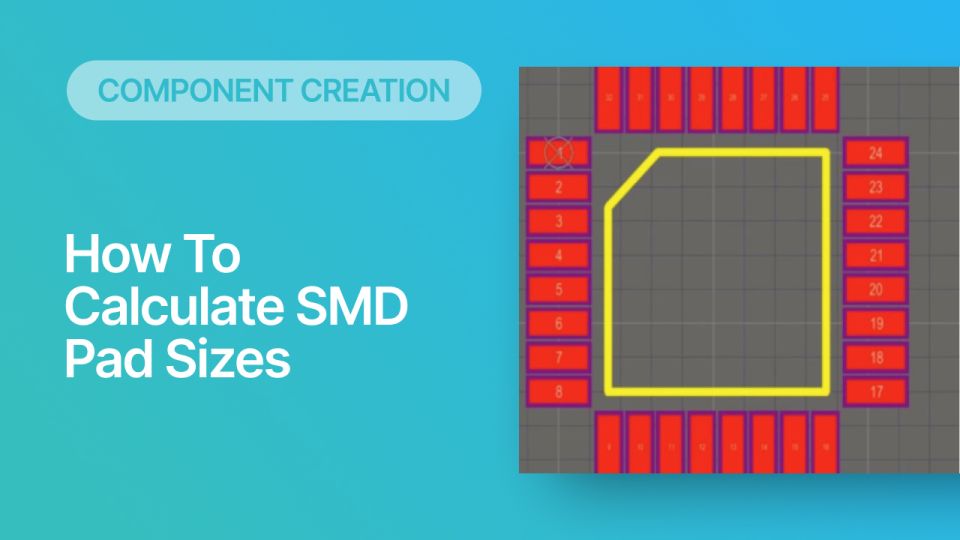
Component creation requires accurate SMD pad sizes in your PCB footprints. See how to determine pad sizes for your SMD components.
Learn how to create footprint with ease using the IPC Compliant Footprint Wizard, built-in to Altium Designer. In this guide, you’ll learn how to quickly create an example SOIC-8 footprint, including automatic generation of an accurate 3D model.
Pro circuit designers don’t just work with components in parallel and series when they design circuits. One way to build
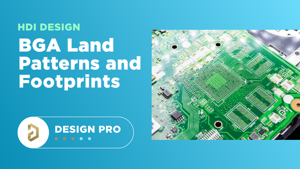
BGA land patterns aren’t always contained in a datasheet. If you need to create one of these, how large do you make the pads, solder mask, and fanout style? Learn more in this article.
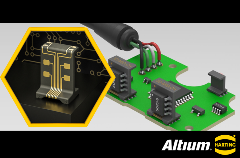
If you’ve ever wanted to mount components vertically, but without the expense of a flex section, use an MID in your PCB.
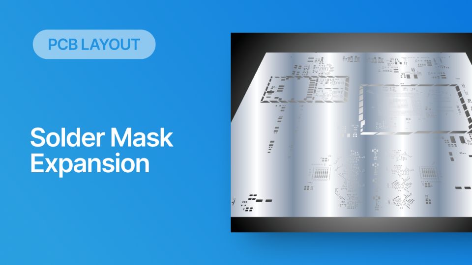
The solder stop mask layer caps off the PCB and provides a protective film over copper on the surface layers
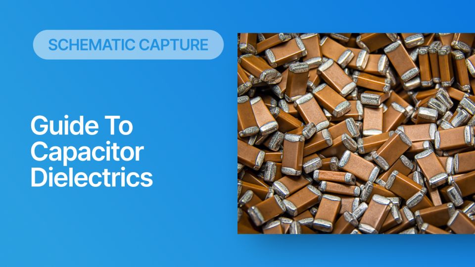
Capacitor electrical behavior is determined, in part, by the capacitor dielectric. Learn all about capacitor dielectrics in this article.