


DDR4/DDR5 설계의 신호 무결성 검증: 길이 매칭에서 전기적 설계 검증으로
길이 일치는 성공적인 DDR 인터페이스를 위한 여러 요소 중 하나일 뿐입니다. 제어 임피던스, 불연속성, 손실 및 기타 레이아웃 효과는 신호 동작에 영향을 미칠 수 있습니다. 제어 임피던스를 포함한 올바른 전기 설계 목표는 표준이나 배선 규칙만으로는 항상 명확하게 드러나지 않습니다.
이번 실습 시간에는 DDR4/DDR5 설계 과정을 살펴보고 PCB 설계 워크플로우 내에서 직접 SI 검증을 수행하는 방법을 보여드리겠습니다.
이 세션은 개별 기능에 초점을 맞추기보다는 엔지니어의 실제 문제 해결 과정을 따릅니다. 즉, 점검해야 할 사항을 파악하고, 분석을 위해 설계를 준비하고, 결과를 검토하고, 그 의미를 이해하고, PCB에서 변경해야 할 사항을 결정하는 과정입니다.
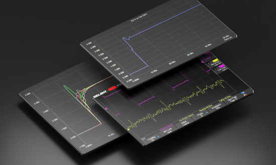
Altium Designer 내에서 Keysight의 신호 분석기를 사용하여 설계가 프로토타입 또는 물리적 검증 단계에 도달하기 전에 통합 분석을 통해 고속 신호에 대한 추가적인 통찰력을 얻는 방법을 시연하겠습니다.
웨비나에서 배울 내용
- DDR4/DDR5 설계에서 중요한 요소를 파악하십시오. 기본적인 라우팅 및 길이 제약 조건 외에 어떤 신호 무결성 문제를 검토해야 하는지 이해하십시오.
- 의미 있는 분석을 위해 설계를 준비하십시오. 스택업, 네트 및 기타 설계 데이터가 분석 품질에 어떤 영향을 미치는지 확인하십시오.
- 분석 결과를 설계 결정으로 전환하세요: 분석 결과를 해석하고, SI 문제의 잠재적 근본 원인을 파악하고, 고려해야 할 PCB 변경 사항을 결정하는 방법을 알아보세요.
- 심층 분석이 필요한 시점을 파악하십시오: 통합 설계 단계 분석이 엔지니어링 의사 결정을 지원할 수 있는 경우와 보다 전문적인 검증 접근 방식이 적절한 경우를 확인하십시오.
참석해야 하는 이유는 무엇일까요?
- 제품 기능 시연보다는 실제 엔지니어링 워크플로를 따르세요.
- 실제 DDR4/DDR5 설계에 적용된 신호 무결성 분석을 참조하십시오.
- 전기 분석 결과를 바탕으로 실행 가능한 PCB 설계 결정을 내리는 방법을 알아보세요
- 전기 분석이 의미를 갖기 전에 필요한 설계 정보가 무엇인지 이해해야 합니다.
- Signal Analyzer가 Altium Designer 설계 워크플로에 얼마나 자연스럽게 통합되는지 확인해 보세요.
- 실시간 Q&A 시간에 직접 질문하세요.
참석 대상
- PCB 설계자는 다음과 같은 작업을 수행합니다. DDR4/DDR5와 같은 고속 디지털 인터페이스
- 보드 레벨 신호 및 전력 무결성을 담당하는 하드웨어 엔지니어
- 설계 프로세스에 전기적 검증을 조기에 도입하고자 하는 기술 책임자 및 수석 엔지니어
- Altium Designer를 사용하는 엔지니어 중 신호 분석기에 대한 실질적인 이해를 원하는 분들을 위한 책입니다.
- 프로토타입 제작 전에 설계 동작 방식을 더 잘 이해하고 후기 단계의 문제 해결에 대한 의존도를 줄이고자 하는 엔지니어링 팀

Author
Author
Alexsander joined Altium as a Technical Marketing Engineer and brings years of engineering expertise to the team. His passion for electronics design combined with his practical business experience provides a unique perspective to the marketing team at Altium. Alexsander graduated from one of the top 20 universities in the world at UCSD where he earned a Bachelor’s degree in Electrical Engineering.

Author
Author
Martin Malenica has a masters in electronic and computer engineering at the University of Zagreb. His previous experience consists of multiple embedded systems positions at robotics start-ups (Gideon with USD 35m in Seed and Series-A funding) and SMEs. His engineering strengths lie in system architecture, PCB design and embedded programming. Aside from engineering, Martin has spent the last 1.5 years working at a leading European management consulting firm, where he focused on strategies to support large OEMs and Tier-1s regarding the current semiconductor shortage across the whole EMEA region. Martin has practical experience within AD, but also a good understanding of competitor tools, especially on the procurement and supply chain side, like Everstream, Resilinc, Silicon Expert, Z2Data etc. Martin Joined Altium in 2023 as part of the Technical Sales team in Germany.
Author
Author
Majdi Thouabtia’s background is in electrical engineering, with several years of experience in hardware development and technical project management. He has worked across the full hardware lifecycle, from EMC-compliant circuit design and PCB layout to prototyping, testing, and production. Throughout my career, Altium Designer has been a key tool in his daily work, so he is especially proud to now be part of the team behind it.
Before joining Altium, he contributed to projects in the EV charging and IoT sectors, leading development efforts and collaborating with cross-functional teams and external partners. He holds a Master’s degree in Electrical Engineering from FAU Erlangen-Nürnberg.

Author
Author
Francesco holds a Master's degree in Electrical Engineering from EPFL, Switzerland. He is currently part of the Field Applications Engineering team at Altium. During his studies, his primary focus was on bioelectronics and the microfabrication of biomedical implants. After graduating, Francesco transitioned into a technical sales role with a global supplier and manufacturer of custom magnetics, where he was responsible for both technical and sales discussions, serving as the liaison between design engineers, manufacturing engineers, and customers.

Author
Author
Aiden은 대학에서 전자공학을 전공하였으며 PCB 설계 분야의 R&D로 7년 이상의 경험을 가지고 있습니다. 그는 전자 제품을 위한 SMPS, 인버터, 컨버터 설계 경험이 있습니다. 제품 프로젝트를 이끌었으며 설계, 관리, 인증 제품 테스트와 같은 모든 작업을 경험했습니다. 그리고 한국 리셀러(Hancom Intelligence) 팀에서 4년 이상 Altium Designer 사용자들을 위한 기술 지원 및 교육을 제공했습니다. Concord Pro와 Altium 365를 사용하여 PLM 요구 사항에 대한 컨설팅 및 지원을 했습니다. 또한 Altium Designer에 대한 수십 차례의 교육 및 웨비나를 경험했습니다.
Aiden은 2022년 11월부터 Altium에서 기술 영업 엔지니어로 근무하고 있으며 현재 한국 사무소에 근무하고 있습니다.

Author
Author
Daniel joined Altium in 2019 as an Application engineer and moved into the Technical Sales role in the same year. Daniel provides technical assistance for sales, third party distributors, and customers in the Asia Pacific region (APAC) and is based in the Altium Tokyo, Japan office. Daniel has experience with PCB, FPGA, and ASIC design in telecommunication and Information industries.


 JUN


CET
결과 없음.
모든 날짜 보기
Registration has recently closed. Check back soon for on-demand webinar.
Related Technical Documentation
관련 자료
DDR4/DDR5 설계의 신호 무결성 검증: 길이 매칭에서 전기적 설계 검증으로
작성 날짜: October 21, 2026

At a Glance
실제 DDR4/DDR5 설계에서 신호 무결성을 조사하고 전기 분석 결과를 실질적인 PCB 설계 결정으로 전환하는 방법을 알아보세요.


Product:
웨비나
Altium Agile Teams
시뮬레이션 및 분석
신호 무결성
PCB 설계 엔지니어
시뮬레이션 엔지니어
길이 일치는 성공적인 DDR 인터페이스를 위한 여러 요소 중 하나일 뿐입니다. 제어 임피던스, 불연속성, 손실 및 기타 레이아웃 효과는 신호 동작에 영향을 미칠 수 있습니다. 제어 임피던스를 포함한 올바른 전기 설계 목표는 표준이나 배선 규칙만으로는 항상 명확하게 드러나지 않습니다.
이번 실습 시간에는 DDR4/DDR5 설계 과정을 살펴보고 PCB 설계 워크플로우 내에서 직접 SI 검증을 수행하는 방법을 보여드리겠습니다.
이 세션은 개별 기능에 초점을 맞추기보다는 엔지니어의 실제 문제 해결 과정을 따릅니다. 즉, 점검해야 할 사항을 파악하고, 분석을 위해 설계를 준비하고, 결과를 검토하고, 그 의미를 이해하고, PCB에서 변경해야 할 사항을 결정하는 과정입니다.
Altium Designer 내에서 Keysight의 신호 분석기를 사용하여 설계가 프로토타입 또는 물리적 검증 단계에 도달하기 전에 통합 분석을 통해 고속 신호에 대한 추가적인 통찰력을 얻는 방법을 시연하겠습니다.
웨비나에서 배울 내용
- DDR4/DDR5 설계에서 중요한 요소를 파악하십시오. 기본적인 라우팅 및 길이 제약 조건 외에 어떤 신호 무결성 문제를 검토해야 하는지 이해하십시오.
- 의미 있는 분석을 위해 설계를 준비하십시오. 스택업, 네트 및 기타 설계 데이터가 분석 품질에 어떤 영향을 미치는지 확인하십시오.
- 분석 결과를 설계 결정으로 전환하세요: 분석 결과를 해석하고, SI 문제의 잠재적 근본 원인을 파악하고, 고려해야 할 PCB 변경 사항을 결정하는 방법을 알아보세요.
- 심층 분석이 필요한 시점을 파악하십시오: 통합 설계 단계 분석이 엔지니어링 의사 결정을 지원할 수 있는 경우와 보다 전문적인 검증 접근 방식이 적절한 경우를 확인하십시오.
참석해야 하는 이유는 무엇일까요?
- 제품 기능 시연보다는 실제 엔지니어링 워크플로를 따르세요.
- 실제 DDR4/DDR5 설계에 적용된 신호 무결성 분석을 참조하십시오.
- 전기 분석 결과를 바탕으로 실행 가능한 PCB 설계 결정을 내리는 방법을 알아보세요
- 전기 분석이 의미를 갖기 전에 필요한 설계 정보가 무엇인지 이해해야 합니다.
- Signal Analyzer가 Altium Designer 설계 워크플로에 얼마나 자연스럽게 통합되는지 확인해 보세요.
- 실시간 Q&A 시간에 직접 질문하세요.
참석 대상
- PCB 설계자는 다음과 같은 작업을 수행합니다. DDR4/DDR5와 같은 고속 디지털 인터페이스
- 보드 레벨 신호 및 전력 무결성을 담당하는 하드웨어 엔지니어
- 설계 프로세스에 전기적 검증을 조기에 도입하고자 하는 기술 책임자 및 수석 엔지니어
- Altium Designer를 사용하는 엔지니어 중 신호 분석기에 대한 실질적인 이해를 원하는 분들을 위한 책입니다.
- 프로토타입 제작 전에 설계 동작 방식을 더 잘 이해하고 후기 단계의 문제 해결에 대한 의존도를 줄이고자 하는 엔지니어링 팀
Related Technical Documentation
관련 자료

대규모에서도 빠른 속도. 체계적인 반복 가능성. 안전한 유연성.
고급 다분야 협업을 위한 통합 플랫폼
Platform-based Solutions
Tools
Platform
Company
Software Capabilities
Contact Us
Careers