Skip to main content
Mobile menu
Discover
Develop
Agile
Resources & Support
Free Altium 365 Tools
Gerber Compare
Online PCB Viewer
Resources & Support
Learning Hub
Support Center
Documentation
Webinars
Altium Community
Forum
Bug Crunch
Ideas
Education
Student Lab
Educator Center
Altium Education Curriculum
Search Open
Search
Search Close
Sign In
Main menu
Home
PCB Design
Collaboration
Component Creation
Data Management
Design Outputs
ECAD/MCAD
HDI Design
High Speed Design
Multi-Board
PCB Layout
PCB Routing
PCB Supply Chain
Power Integrity
RF Design
Rigid Flex
Schematic Capture
Signal Integrity
Simulation
Software
Develop
Discover
Agile
Altium 365
Altium Designer
Education
Programs
Altium Academy
Engineering News
Guide Books
Newsletters
Podcasts
Projects
Training Courses
Webinars
Whitepapers
Altium Designer 19 vs Altium Designer 18 Feature Comparison
Read Article
1:06
Unified Design Environment - Benefits:PCBWorksvid
Watch Video
Designing a 6-Layer PCB Stackup for Enhanced EMC
6-layer PCBs are an economical and popular stackup for a variety of applications with high net count and small size. Larger boards might work fine with a 4-layer stackup, where signal layers can be sacrificed to ensure isolation between each side of the board. With the right 6-layer stackup, you can suppress EMI between different layers and accommodate fine-pitch components with high net count. However, there are cases where it makes more sense
Read Article
Tips for High Frequency PCB Design in Embedded Systems
Today's high-speed embedded systems incorporate diverse functionality, components, digital interfaces, and of course, wireless/RF signaling. If you're designing embedded systems with any level of computing power that also includes an analog front end, then you have multiple mixed-signal design challenges to overcome. Whether it's a simple sub-1 GHz radio connection, Wifi/BLE, or multi-gigabit Ethernet, embedded systems need some way to interface
Read Article
DFSI: Overcoming Channel Loss
In a previous article, we established that loss is one of the primary signal integrity challenges to overcome. In this article, we’ll talk about the sources of loss, what you can do about them, and an often neglected aspect of loss. There are various options for reducing loss, in this article I’ll discuss how to: Change your architecture to orthogonal or cables Use better PCB materials with lower DF resin and smoother copper Add active repeaters
Read Article
Design for Reliability with Yizhak Bot
Design for Reliability. In this episode learn from Yizhak Bot what derating is and how you can work on the schematic level with their simulation software to eliminate field failures. Watch it here.
Read Article
Weekly Digest: Preparing for IPC-6012E
This week HDI expert Happy Holden reported on an important issue related to the upcoming IPC-6012E, Qualification and Performance Specification for Rigid Printed Boards in his article, The IPC Warning About Microvia Reliability for High Performance Products. Learn more about this warning regarding field and latent failures of high-profile HDI boards and what you can do if you want to get involved or get more information. Access Happy’s article
Read Article
5:33
Top 5 reasons to upgrade
Watch Video
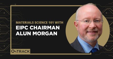
Materials Science 101 with EIPC Chairman Alun Morgan
How to choose materials? Talk to your manufacturers about the correct materials for your PCB Design, or click here to watch Judy Warner's interview with the materials scientist, Alun Morgan.
Read Article
40:17
Altium Designer 19: Advanced Layer Stack Manager
Watch Video
Pagination
First page
« First
Previous page
‹ Previous
…
Page
233
Page
234
Page
235
Page
236
Current page
237
Page
238
Page
239
Page
240
Page
241
…
Page
250
Page
260
Page
270
Page
280
Page
290
Page
300
Page
310
Page
320
Page
330
Page
340
Next page
Next ›
Last page
Last »
Subscribe to