Skip to main content
Mobile menu
Discover
Develop
Agile
Resources & Support
Free Altium 365 Tools
Gerber Compare
Online PCB Viewer
Resources & Support
Learning Hub
Support Center
Documentation
Webinars
Altium Community
Forum
Bug Crunch
Ideas
Education
Student Lab
Educator Center
Altium Education Curriculum
Search Open
Search
Search Close
Sign In
Main menu
Home
PCB Design
Collaboration
Component Creation
Data Management
Design Outputs
ECAD/MCAD
HDI Design
High Speed Design
Multi-Board
PCB Layout
PCB Routing
PCB Supply Chain
Power Integrity
RF Design
Rigid Flex
Schematic Capture
Signal Integrity
Simulation
Software
Develop
Discover
Agile
Altium 365
Altium Designer
Education
Programs
Altium Academy
Engineering News
Guide Books
Newsletters
Podcasts
Projects
Training Courses
Webinars
Whitepapers
Wearable Design: Why Fashion, Function and PCB Form Factor Matter
Fashion meets function in wearables. Learn how PCB form factors and structural electronics enable sleek, user-friendly, high-performance designs.
Read Article
DRCs in PCB Design: How They Can Save Your Design from Sinking
For many years I owned a small boat which gave me hours of fun on the water, but there are a few critical rules that have to be obeyed. One of those rules is that you MUST install the drain plug before putting your boat in the water. It’s a lot cheaper to go for a swim intentionally, rather than unexpectedly in order to retrieve your new boat. Everyone knows that rules are there for our protection. But sometimes, whether accidentally or on
Read Article
Considerations for Designing a High Voltage PCB
I used to think that high voltage applications were only used in power engineering. Since I had no desire to work at a power plant or transformer station, I was safe from having to learn high voltage PCB design considerations. Alas, my interest in space applications proved me wrong and forced me to confront my laziness. It turns out high voltage applications show up in almost every industry, from manufacturing and power plants to medical and
Read Article
Assessing the Post-Development Hardships of Uncontrolled Data Management
For every, team, and business, getting to the release state should be the moment where you can breathe a sigh of relief. This moment, unfortunately, doesn’t always lend itself to joyful celebration. Project completion can mean a) you and your team have successfully constructed a design without any flaws in the documentation process and can now prep for its release, or b) you’ve successfully completed your design but realize a minor (or major)
Read Article
IoT Resource Bundle
From the early days of printed circuit boards, the electronics industry has made huge strides in board materials, copper printing methods, miniaturization, rigid-flex, ELIC, EDA, and much more. Many of the devices we use in our homes, our vehicles, and in our workplaces would not be possible without this continuous evolution of PCB design and technology. The scope of creativity from individuals is unbounded. While the infrastructure for IoT can
Read Article
RF Technologies for Low-Power Wireless Communications: Ambient Backscatter
I love family reunions, though, with forty people in my extended family they can get a bit hectic. Whether we’re playing cards, swimming, or at the dinner table there’s always someone telling jokes and stories. In fact, most people are trying to talk so sometimes you have to yell to be heard. It can also be difficult to communicate in the electromagnetic spectrum. Your devices often have to “shout” their own signals into the void in order to
Read Article
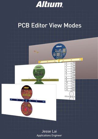
PCB Editor View Modes
PCB editor view modes allow designers to locate and correct errors in particular areas of the board. Altium Designer features multiple ways to view your design, allowing you to be most efficient and to help avoid errors. These different PCB editor view modes have allowed users to find and fix design problems, such as why a flex board does not fold, why components are on the wrong layers, and why dead copper is not being shown anywhere on the board
Read Article
How to Prevent Hairline Short Circuits in Your PCB Circuit Design
What’s worse than finding a strand of hair in your pasta when you’re out on a dinner date? Finding it after it has ended up in your mouth. There are two ways to avoid awkward scenarios like this. For one, you can keep a close eye on your food and make sure it is hair free before it enters your mouth. The second is to ensure that there is no chance of a hair ending up in your food; in this case, you might need to go to a new restaurant. In PCB
Read Article
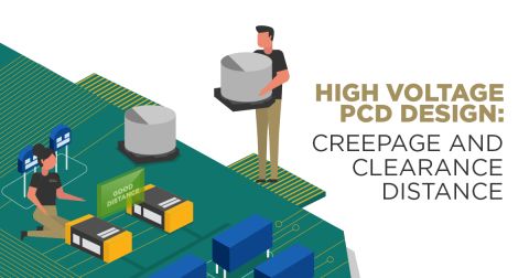
High Voltage PCB Design: Creepage and Clearance Distances for High Voltage
Designing high voltage PCBs following specific spacing guidelines is critical. In high density circuit boards, spacing is even trickier and more important for protection.
Read Article
Capturing Key Design Details in PCB Documentation
One of the most important yet often avoided aspects of documenting a design is the formal design document. Too often we finish the design, generate fabrication, assembly, and validation documents then consider the job done. Properly capturing the system specification, design intent, design process and traceability back to the specification is a time-consuming and arduous yet very necessary task. The design document must capture all aspects of the
Read Article
Pagination
First page
« First
Previous page
‹ Previous
…
Page
337
Page
338
Page
339
Page
340
Current page
341
Page
342
Page
343
Page
344
Page
345
…
Page
350
Page
360
Page
370
Page
380
Page
390
Page
400
Page
410
Page
420
Next page
Next ›
Last page
Last »
Subscribe to