Skip to main content
Mobile menu
Discover
Develop
Agile
Resources & Support
Free Altium 365 Tools
Gerber Compare
Online PCB Viewer
Resources & Support
Learning Hub
Support Center
Documentation
Webinars
Altium Community
Forum
Bug Crunch
Ideas
Education
Student Lab
Educator Center
Altium Education Curriculum
Search Open
Search
Search Close
Sign In
Main menu
Home
PCB Design
Collaboration
Component Creation
Data Management
Design Outputs
ECAD/MCAD
HDI Design
High Speed Design
Multi-Board
PCB Layout
PCB Routing
PCB Supply Chain
Power Integrity
RF Design
Rigid Flex
Schematic Capture
Signal Integrity
Simulation
Software
Develop
Discover
Agile
Altium 365
Altium Designer
Education
Programs
Altium Academy
Engineering News
Guide Books
Newsletters
Podcasts
Projects
Training Courses
Webinars
Whitepapers
3D PCB Design
When it comes to designing circuit boards, you know that being able to properly visualize your spacing, sizing, and layout is crucial to a successful finished product with minimal setbacks. While standard PCB design software has its place, 3D PCB software allows you to get a detailed look at your routing, components, and overall layout BEFORE you send your design out for a physical prototype. As 3D environments become more advanced, they become
Read Article
PCB Design Techniques to Reduce EMI
Reduce EMI in your PCB designs. This presentation will discuss multiple ways good PCB design can help manage EMI interference on your board. It covers tips and tricks for basics and beyond, including: using EMI cans for shielding, proper grounding techniques, trace length, isolating AC and DC signals and differential pair routing. Click the PDF above to read more about PCB design techniques to reduce EMI in this presentation. Or view the original
Read Article
How to Work with Your PCB CAD Software Support Technicians
Have you ever been in a situation where you are trying to help someone, but they don’t understand what you are talking about? You want to help them through their difficulties, but the two of you seem to be from different worlds. If that scenario doesn’t sound familiar to you, then you’ve probably never raised teenagers. If it does ring a bell, then you may be a seasoned parent, or you may even be a customer support technician. I firmly believe
Read Article
Essential PCB Design Tips: How to Implement a Watchdog Timer in Your PCB Design
When you work from home there are some perks of the job. You can make your own meals, slot in some laundry over lunch, and drink all the tea you want. I use a stove-top kettle to boil water for my tea, so when I get in the writing zone, I rely on its high-pitched whistle to tell me when it’s done. Sometimes when I’m careless, I don’t fit the lid on properly. As a result, the kettle remains silent despite the fact that the liquid water inside of
Read Article
The Top Reasons Why PCB Design Software with Auto Routing Can Save You Time
I’ve been designing printed circuit boards long enough that my family has sadly grown accustomed to me spending more time at work than at home. When deadlines are looming, everyone knows I’ll be working late nights at the office. Modern PCB design software with auto-routing tools can help you cut down your routing time, but not everyone is a fan of these features. I know all the arguments against using an auto-router because I’ve been using them
Read Article
PCB Design: An Optocoupler Tutorial for Your PCB Layout
Are you guilty of hitting the snooze button at least twice before you reluctantly wake up from your blissful sleep? My wife claims that I probably have the world record time for hitting the snooze button since I do it without even opening my eyes. But there are times when the third snooze alarm mysteriously doesn’t go off and it is a losing battle to get my day started on time. In electronics, embedded systems often rely on optocoupler circuits
Read Article
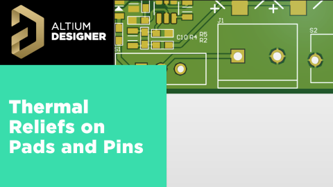
Thermal Relief Guidelines for PCB Layout
Sometimes, thermal reliefs are a DFA measure for a new PCB. Here’s when you should use thermal pads in a PCB.
Read Article
3D PCB Design
3D PCB Design takes board design to the next level, especially when it comes to Multi-board system design. Learn tips and techniques to approach 3D PCB design that will help you take your unified design process to the next level. Being able to properly visualize your spacing, sizing, and layout is crucial to success. Learn more from this 3D PCB Design presentation, and click the PDF above to read more in this presentation overview. Or view the
Read Article
PCB Layout
Become an expert in PCB Layout when you use Altium Designer software. Benefits to the Unified Data Model Approach include not just time savings, but the potential of simultaneous design that is available with the integrated schematics and PCB layouts offered in Altium Designer. Simultaneously consider the big picture and the very details that impact your projects' success. Click the PDF above to read more about PCB Layout in this presentation
Read Article
Protect Your PCB From ESD
From computers and televisions, to automobiles and kitchen appliances, PCBs are found in nearly every aspect of our lives-- many of our devices would not be possible without them. They are the brains of our electronics, and as such, it is of the utmost importance to do everything in our power to ensure our designs are protected from potentially catastrophic threats. Proper routing and schematics, component placement, and special attention to
Read Article
Pagination
First page
« First
Previous page
‹ Previous
…
Page
323
Page
324
Page
325
Page
326
Current page
327
Page
328
Page
329
Page
330
Page
331
…
Page
340
Page
350
Page
360
Page
370
Page
380
Page
390
Page
400
Page
410
Page
420
Next page
Next ›
Last page
Last »
Subscribe to