Skip to main content
Mobile menu
Discover
Develop
Agile
Resources & Support
Free Altium 365 Tools
Gerber Compare
Online PCB Viewer
Resources & Support
Learning Hub
Support Center
Documentation
Webinars
Altium Community
Forum
Bug Crunch
Ideas
Education
Student Lab
Educator Center
Altium Education Curriculum
Search Open
Search
Search Close
Sign In
Main menu
Home
PCB Design
Collaboration
Component Creation
Data Management
Design Outputs
ECAD/MCAD
HDI Design
High Speed Design
Multi-Board
PCB Layout
PCB Routing
PCB Supply Chain
Power Integrity
RF Design
Rigid Flex
Schematic Capture
Signal Integrity
Simulation
Software
Develop
Discover
Agile
Altium 365
Altium Designer
Education
Programs
Altium Academy
Engineering News
Guide Books
Newsletters
Podcasts
Projects
Training Courses
Webinars
Whitepapers
1:43
Adding Net Labels - EvalQuest
Watch Video
8:19
How Do I Annotate My Design - EvalQuest
Watch Video
3:00
Exploring The Workspace - EvalQuest
Watch Video
5:49
Working With Panels - EvalQuest
Watch Video
3:50
Creating A PCB Project - EvalQuest
Watch Video
3:31
Setting Options And Preferences - EvalQuest
Watch Video
1:34
Evaluation Guide Intro
Welcome to the Altium Designer Evaluation Guide! We’d like to congratulate you on taking the first step towards learning how to use Altium Designer. There’s a lot to learn, so strap yourself in for a rewarding journey. If you’re completely new to Altium Designer, then you might find some differences when compared with your current PCB design tool. Altium Designer combines the overarching design process into one seamless, unified design experience
Watch Video
Design Prep: Centralizing Your Design Data
Electronics design, like cooking, requires having the right ingredients in place to complete your creations. What if all that information was located in a single, centralized location so that everyone in the organization had access to pre-defined, pre-approved design ingredients to speed the process? Read on to learn more. I really like cooking. The satisfaction of tinkering with a recipe, and getting the flavors and balance just right. The
Read Article
How to Maximize Copper in Your PCB Design: The Pros and Cons of Copper Pouring Versus Placing
Image Source: Flickr user billautomata ( CC BY 2.0) There is a saying in copper pour PCB layout, “Copper is free.” It means a printed circuit board editor designer must think in reverse. A circuit board starts off as solid copper, and the copper you don’t want is removed. It is faster to build, less consumptive, and less expensive to make a printed circuit board that is mostly copper as compared to the same size board that is mostly bare. Picking
Read Article
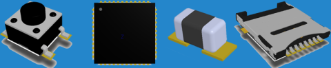
PCB Design: Create 3D Component in a Footprint Library
In today’s PCB design process, your design and CAD tool needs to be able to integrate mechanical design workflows into an electrical design tool. Read on to learn how to create 3D component bodies in a footprint library. In today’s PCB design process, you need to be able to integrate mechanical design workflows into an electrical design tool. Transferring inaccurate design data back and forth between the ECAD and MCAD worlds not only causes
Read Article
Pagination
First page
« First
Previous page
‹ Previous
…
Page
384
Page
385
Page
386
Page
387
Current page
388
Page
389
Page
390
Page
391
Page
392
…
Page
400
Page
410
Page
420
Next page
Next ›
Last page
Last »
Subscribe to