


How to Select GaN FETs for RF and Automotive Applications

At a Glance
Learn how to select GaN FETs for RF and automotive applications, including key specs, performance benefits, and design considerations. Discover GaN FETs advantages and explore example applications on Octopart!


All electronics need some level of power conversion, regulation, and conditioning, but talks of efficient power have never been more at the forefront of discussion in advanced technology. Power delivery and conversion considerations used to center more around noise and heat, whereas today, these considerations now focus on tailored strategies for advanced systems. Whenever you have needs for power conversion, you also need to ensure the lowest possible heat dissipation as this is critical to device reliability.
In wireless systems, achieving high power efficiency with minimal thermal loss is critical for power amplifier and transmitter stages. For these specialized components, engineers often consult the RF & Microwave components category. Historically, the industry faced significant heat management problems in RF delivery, a challenge that now extends to automotive power management. These sectors require innovative solutions for high-density power delivery.
What Are GaN FETs?
GaN FETs (Gallium Nitride Field-Effect Transistors) provide a breakthrough solution due to their extreme power limits, high-frequency capabilities, and superior thermal conductivity into an SiC or Si substrate. Engineers can explore the latest options in Power Transistors to find GaN-based solutions. As these models become more accessible from global distributors, selecting the right part involves balancing specific automotive and RF constraints.
Why Use GaN FETs in RF and Automotive Applications?
GaN FETs are High Electron Mobility Transistors (HEMTs). Their material properties make them superior to legacy silicon for high-switching frequencies and high-voltage output. When evaluating wide bandgap semiconductors, the following characteristics provide a distinct advantage:
-
Breakdown field: GaN has a higher breakdown electric field than Si (approximately 15x as large as that in Si), so a GaN device can be operated at higher voltages than an Si MOSFET of the same size.
-
Electron mobility: The electron mobility of GaN is higher than that of Si, so a GaN transistor can be physically smaller than an Si transistor with the same R_ON resistance.
-
Thermal conductivity: GaN has a higher thermal conductivity than Si (approximately 2x as large), so it can more efficiently dissipate heat into its substrate or a heatsink.
-
Capacitances: The capacitances between inputs on a GaN FET are smaller to those in an Si MOSFET when the two devices have approximately the same physical size.
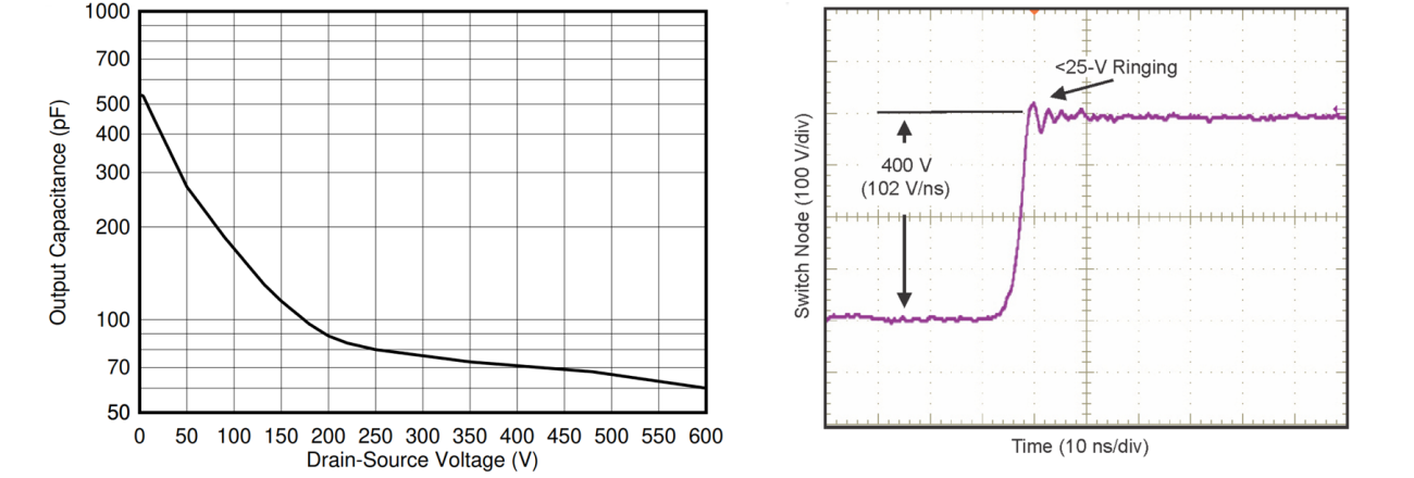
There are two common varieties of GaN FETs: those grown on Si and those on SiC. The thermal conductivity of SiC is approximately 170% of that for GaN, so GaN FETs formed via heteroepitaxial growth of GaN on SiC are preferred in high power applications. For switching applications, such as high power switching regulators, the possibility of lower capacitances and smaller R_ON values enables very fast power delivery, with rise times on the order of nanoseconds.
These characteristics mean that a GaN FET can generally be run at a high frequency and higher power simultaneously, both of which are needed in power electronics for RF and automotive applications. The primary concern in automotive is power regulation and delivery to an electromechanical system (the motor), while the concern in RF systems is high-efficiency power regulation and delivery to a transceiver and power amplifier. There are other applications in power conversion where, one could argue, the same characteristics would provide benefits. For example, upcoming clean energy systems can take a cue from RF systems and implement the same topologies used for power conversion and charging/discharging in energy storage.
At this point, let’s dig deeper into multiphased power conversion to see some of the main operating requirements for GaN FETs in advanced automotive and RF power systems.
High Frequency Power Conversion Benefits
When we say “high frequency” in terms of power conversion, we’re referring to the switching frequency generally used in a PWM driver or, less commonly, a PFM driver in a switching converter. If you’re familiar with switching converters, then you know that switching losses in a MOSFET can be reduced when the driving component can switch between states faster (lower rise time). In addition, a MOSFET that can run at higher modulation frequencies will produce lower ripple on the output voltage/current. It also allows system size to be reduced as a smaller inductor would be needed in order to hit a specific ripple target. For systems where these constraints are particularly tight, designers may implement multiphase architectures using Power Management ICs / Controllers.
An appropriately sized GaN FET can meet these requirements as long as the peak transient voltage, transient current, and switching time specifications can be balanced for a given switching frequency. In the event these three specifications can’t be compromised, a design can be run in a multiphase configuration, where the converter operates with multiple stages in parallel, but separated by equal phases. In this way, the converter mimics a higher frequency converter. Within each stage, multiple parallel arrangements of GaN FETs can be used to deliver very high current as needed.
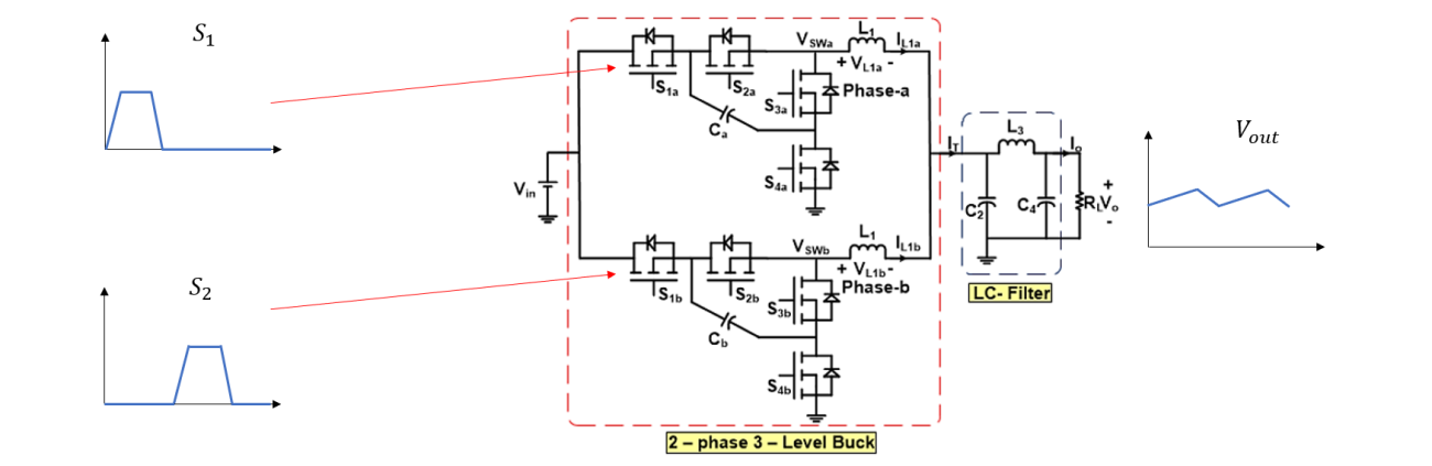
Running in multiphased operation in this way requires careful component selection on the output portion of each stage. For RF systems, these designs should run up to very high frequencies of ~10 MHz or more. This selection as well as an output filtering and control stage can be used to ensure the output power follows the envelope imposed on the output voltage/current waveform by the baseband signal. To prevent unwanted ringing or oscillations between different stages, a high voltage diode is normally used, just as you would with in-phase parallel arrangements of MOSFETs supplying current simultaneously. The controller and driver stage in this type of design need to be carefully selected such that they can sufficiently modulate the GaN FETs while also operating within a control loop to compensate for any overvoltage or dropout during operation.
Key GaN FET Specifications to Consider
For the important application areas outlined here, there are four main specifications that should receive attention during design and component selection:
-
Peak drain-to-source voltage (DC and transient): These values here are needed for DC power delivery with smooth turn-on, or regulation as a switching element with fast turn-on. Note that transient peak voltage will be specified for a specific pulse time
-
Peak current (DC and transient): Just like peak voltage values, the transient value will be specified with a specific pulse time corresponding to the length of the output pulse.
-
Gate voltage: Typical gate voltages will be listed in the component datasheet, make sure to check these so a GaN FET can be driven with the appropriate gate driver. Typical gate voltages can be in the 10 to 20 V range for ~500-600 V DC peak GaN FETs with high current handling.
-
Dynamic switching times: These specifications include turn-on delay, rise time, and reverse recovery time for the body diode. For GaN FETs, these values are on the order of 10-100 ns thanks to the lower load capacitance of these systems.
-
Input/output capacitances: Parasitic capacitances on the input and output ports of the device are also important as they will determine the interaction with inductive loads, possibly leading to underdamped ringing in the case where the load has low resistance. Typically it’s sufficient to add in a small resistor to critically damp any transition on the switching node.
Watch out for the input and output capacitances in any power MOSFET, including a GaN FET, when driving an inductive load. In particular, don’t think that you can just regulate away ringing at a switching node through a feedback loop and a control algorithm. Your gate driver IC will likely be unable to compensate for this ringing, unless you’ve implemented control in a fast MCU or FPGA, which is excessively costly. Instead, you can run these devices at higher frequency and use a smaller inductor, which will still help you hit your ripple target.
Example GaN FET and Gate Driver Solutions
Nexperia, GAN063-650WSAQ
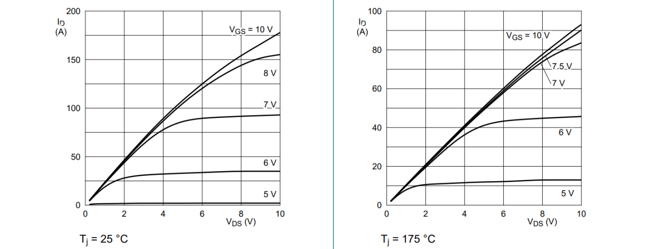
The GAN063-650WSAQ from Nexperia is an excellent example of a general-purpose GaN FET. This component switches with up to 20 V gate voltage with a fast turn-on time of 57 ns (10 ns output rise time). At only 10 V gate voltage, this FET provides 34.5 A in DC, with peak transient current of 150 A with fast pulsing of less than 10 microseconds. ON-state resistance is only 50 mOhms at room temperature, and only rises up to 120 mOhms at 175 °C. Peak DC drain-source voltage in this component reaches 650 V. The output drain current characteristics are shown below.
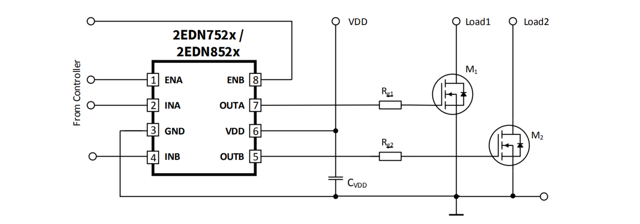
Infineon, 2EDN7524FXTMA1
The 2EDN7524FXTMA1 from Infineon is a gate driver IC that can be used with GaN FETs. This component provides 5 ns fast slew rates and 17 ns propagation delay for fast GaN switching, making it useful in switching regulators in RF systems. This component is a dual-channel driver that can interface with a digital controller ASIC. Output voltages reach up to 20 V with typical rise times of 5.3 ns (10 ns maximum, 1.8 nF load capacitance, 12 V drain voltage).
Other Components for Systems With GaN FETs
GaN FETs are one of the important building blocks for power regulation and delivery in RF power systems and automotive power systems. However, you’ll need other components to build your system and ensure reliable power regulation. Some of the other components you’ll need for these systems include:
- RF Front-End: High-performance wireless stages found in RF & Microwave components.
- Signal Isolation: Essential for safety in high-voltage automotive systems, found in Optocouplers.
- Precision Monitoring: Monitoring high-speed power rails using Current Sense Amplifiers.
When you need to find the newest GaN FETs and supporting components for power systems, use the advanced search and filtration features in Octopart. When you use Octopart’s electronics search engine, you’ll have access to up-to-date distributor pricing data, parts inventory, and parts specifications, and it’s all freely accessible in a user-friendly interface. Take a look at our integrated circuits to find the electronics components you need.
Stay up-to-date with our latest articles by signing up for our newsletter.
About Author
Related Resources
Related Technical Documentation
Table of Contents
Design to Release, Without the Friction
- Keep reviews tied to the right version
- Reduce handoff confusion and rework
- Spot sourcing and release risk earlier
- Work solo, share when needed
Get Started
Thank you, you are now subscribed to updates.