


Migration Guide Making the Switch from PADS to Altium Designer Duplicate


THE ALTIUM DESIGNER PHILOSOPHY
At the core of Altium Designer® is one central theme - a unified approach to PCB design software. You’ll find that our tool differs from many conventional alternatives in its approach to design. Our workflow unifies all of the separate yet connected elements required to successfully complete a PCB design.
As an existing PADS user, you are likely used to having multiple tools and interfaces for each stage of your design process. And while each tool excels in its own specialized task, at the end of the day you’re left to manage and remember multiple interfaces, workflows, and methodologies. The question we’ve asked throughout the years is simple - is this approach to Printed Circuit Board design effective?
When we first created Altium Designer, we wanted to create a unified design experience that kept the engineer in complete control of their efficiency and workflow throughout the entire design process. Achieving this goal required us to understand what a complete PCB design software experience entailed for the everyday engineer. As part of the unified approach to PCB design, we connected the following processes into one interface in Altium Designer:
- Schematic Capture
- Board Layout
- Data Management
- Rules and Constraints
- Bill of Materials
- Supply Chain Integration
- Engineering Change Management
- MCAD Collaboration
- Manufacturing Documentation Outputs
With all of these elements integrated in a unified interface, switching back-and-forth between tasks is as simple as selecting the appropriate file to work on in your design workspace. The unified interface then handles all the rest and provides the tools you need for the particular task at hand.
From our more than 30 years of PCB design research and development, we have found that a unified approach to Printed Circuit Board design is the most efficient way to design electronics. This philosophy extends not just to the individual engineer, but also to an entire design team. Projects can easily be worked on by multiple engineers in the same interface, and no time is wasted translating design data back and forth between design environments.
While many have labeled our approach to PCB design the “Altium Way,” we consider it to be the best way to design advanced electronics right the first time.
We hope you enjoy your journey into the world of Altium Designer.

David Cousineau, Sr Field Applications Engineer & The Altium Designer Team
Making a Smooth Transition to Altium Designer Develop from PADS Layout
In this guide, we’ll focus on importing PADS Layout PCB designs. Please refer to specific guides if you need to migrate other files.
Legacy Translation
Before You Begin
This guide will show you how to import data from your legacy system into Altium Designer Develop. Before importing all of your legacy data, it’s important to ask yourself, “why do I need to import my legacy data?” Below are some of the most common considerations to consider when deciding whether to import legacy data into Altium Designer Develop.
"We have 20 years of data, and I don’t want to leave it behind.
- Does the legacy data include critical information for creating robust designs within Altium?
- Is it easier to start new designs rather than re-work the imported data to make it usable?
"Our service bureau doesn’t use Altium, but they can import Altium data. Our Altium system can import their data. Is this a reliable way to pass designs between our companies?.
- How do you maintain library integrity?
- Who has design authority?
- How do you plan to verify the data?
"We have some ‘golden’ designs that we need to bring into Altium Designer Develop so that we can up-issue them.
- How do you plan to verify the imported data?
- How much re-work is going to be needed after importing?
- You need to take advantage of additional Altium Designer Develop features once the data is imported?
"We have a library of trusted parts which we’d like to bring into Altium.
- Are there any exotic parts that you may have trouble representing within Altium?
- Do you need to add Altium-specific features (like 3D models) for every part?
- How much redundancy, duplication, and error is present in your library?
After reviewing these considerations, read on to learn how to import your legacy data into Altium Designer Develop.
Preparing to Migrate Your Legacy Data
There are four phases to migrating legacy data.
1. Prepare original data
|
2. Export data
|
3. Import data
|
4. Post import
|
Phase 1: Prepare Original Data
It is prudent to clean up your design before attempting to export. Below is a checklist of data cleanup best practices to help you as you prepare your data:
Schematic considerations:
- Individual pin connectors (example: Block connectors) in PADS must be modified at PADS tool level before migration. Alternatively, you can replace pin connectors in Altium Designer Develop post-migration.
- Connectors should be represented as one-gate-per-pin with over 256 “gates.”
- Ambiguous connectivity for reuse blocks must be broken apart in PADS.
- Remove hidden pins or implicit connections.
- Local net names placed at wire intersection must be placed at correct locations (away from intersection point)
- Are schematic symbols mapped to correct PCB footprints or not?
- Schematic and PCB are in sync?
PCB considerations:
- Large numbers of graphical objects like mechanical drawing or non-ECO-registered drawing primitives must be migrated on documentation layers.
- Star point grounding check.
- Remove deliberate DRC violations.
- Remove objects extending beyond the environment.
- Known PCB layer assignments need to map correctly with existing Altium Designer Develop PCB, especially with the power plane or signal layer.
- Do the auto-named nets match with the schematic?
Library considerations:
- Do the schematic symbols match with PCB footprints?
- Does the library contain correct supply chain information and BoM parameters?
- Does 3D information need to be imported? If yes, then the height attribute should be assigned in PADS.
- Correct representation of custom pads, copper shapes, solder mask, and resist?
Phase 2: Save Data in a Suitable Format
Supported Version and File Format
The following table shows PADS PCB Design Formats and versions that can migrate into Altium Designer Develop. This list is updated regularly, so please check with us before starting a new migration. Refer to this link for updated information.
| TYPE | SYSTEM | VERSION | FORMAT |
| PCB | PADS Layout | 9.3 | ASCII (.asc) |
| Schematic | PADS Logic | 9.3 | ASCII (.txt) |
| PCB Decal Library | PADS PCB Library | 9.3 | ASCII(.D) |
| Schematic Part and CAE | Decal Library PADS Schematic Library | 9.3 | ASCII Parts (*.P + *.C) |
The Altium Designer Develop Import Wizard can translate PADS schematic, layout, and library data. However, all data must first be exported from PADS as ASCII data.
- To export PADS Logic and Layout data, use the have File » Export menu selections.
- To export library data into ASCII format, use the PADS Library Manager.
- Choose the desired library type (Decals, Parts, Logic)
- Select which items are to be exported, and click the Export button.
- TDecal libraries will export to a *.D file. Parts will export to a *.P file. Logic (CAE) will export to a *.C file.
Layout/PCB and Schematic files translate to Altium Designer Develop as follows:
| PADS FILE TYPE SYSTEM | ALTIUM DESIGNER DEVELOP FILE TYPE |
| PADS Layout/PowerPCB ASCII (*.ASC) | Altium Designer Develop PCB files (*.PcbDoc) |
| Schematic sheets ASCII file (*.TXT) | Altium Designer Develop Schematic file (*.SchDoc) Each schematic sheet will create a separate *.SchDoc file. |
Schematics and PCB files will grouped be and placed in an automatically-created Altium Designer Develop project (*.PrjPCB).
For more information on linking files together to allow for cross navigation and ECO generation, check out the “Component Links” section in our ‘Bringing Together Imported Schematic and PCB Designs’ guide.
Library files translate as follows:
| PADS FILE TYPE | ALTIUM DESIGNER DEVELOP FILE TYPE |
|
PADS Schematic Library ASCII (*.C+*.P) The *.C file contains the graphical portion of a schematic component The *.P file contains the specific part information (pin information, default reference designator, parameters/attributes, footprint/decal pointers, etc.) |
Altium Designer Develop Schematic library files (*.SchLib) |
| PADS PCB Library ASCII (*.D) | Altium Designer Develop PCB library files (*.PcbLib) |
Phase 3: Import Data into Altium Designer Develop
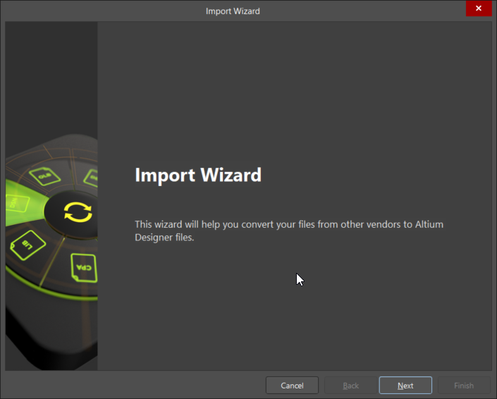
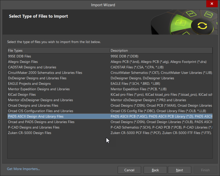
Using the Import Wizard for PADS Files
You can launch the Altium Designer Develop Import Wizard from the File menu.
- Choose the PADS ASCII Design And Library Files option, as shown below.
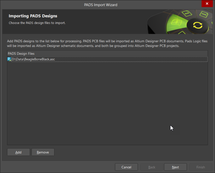
- On the “Importing PADS Designs” screen, click the Add button to choose Layout or Logic files.
- Use the filter button at the bottom right of the file browser to switch between *.ASC and *.TXT files.
- You can translate multiple files at the same time.
- Step-by-step instructions on using the Import Wizard follow next.

Starting the Import Wizard for PADS Files
Step-by-Step Import Instructions for Importing a PADS PCB Design file
- Start the Import Wizard with File » Import Wizard
- Select Type of Files to Import—>PADS ASCII Design And Library Files.
- Add the file(s) to be translated. In this case, a “DEMO.asc” (Layout) file has been selected.
NOTE:
You can add as many .txt and .asc at this point. In the file browser, change the file types pull-down to choose .asc or .txt files, depending on what you want to import. However, if you add files of a different file name, Altium Designer Develop will create separate projects.
- Add any Schematic or PCB Libraries to import (if available).
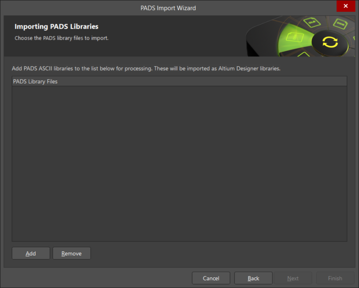
NOTE:
Because the library part and decal information is included in the source files, it is unnecessary to add libraries for schematic or PCB files to translate successfully. Only add libraries to this screen if you wish to translate entire libraries for later use in Altium Designer Develop independently.
- Before PCB files are translated from PADS to Altium Designer Develop, Altium Designer Develop will analyze them to determine how to map the PADS layer definitions in Altium Designer Develop. You can adjust your layer mapping manually if desired. You can also set PADS layers not to import if you don’t need information from that layer in your Altium Designer Develop project.
- Specific to Internal layers:
- PADS inner signal layers will be initialized as Altium signal layers (e.g., “Mid Layer 1”)
- PADS CAM Plane layers will be initialized as Altium Plane Layers (e.g., “Internal Plane 1”). These are negative-image planes similar to PADS CAM planes.
- PADS inner layers defined as Split/Mixed layers will be initialized as Altium signal layers if any trace or other positive image electrical data is present. If the Split/Mixed layer only has pour shapes, it will be initialized as an Altium Plane layer and imported with all split, embedded, and isolated plane areas intact.
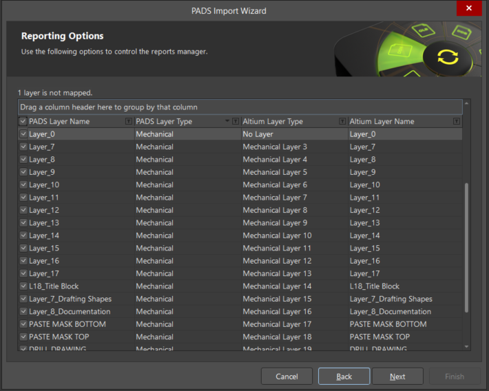
- Set the options for what level of reporting is needed after the translation is complete.
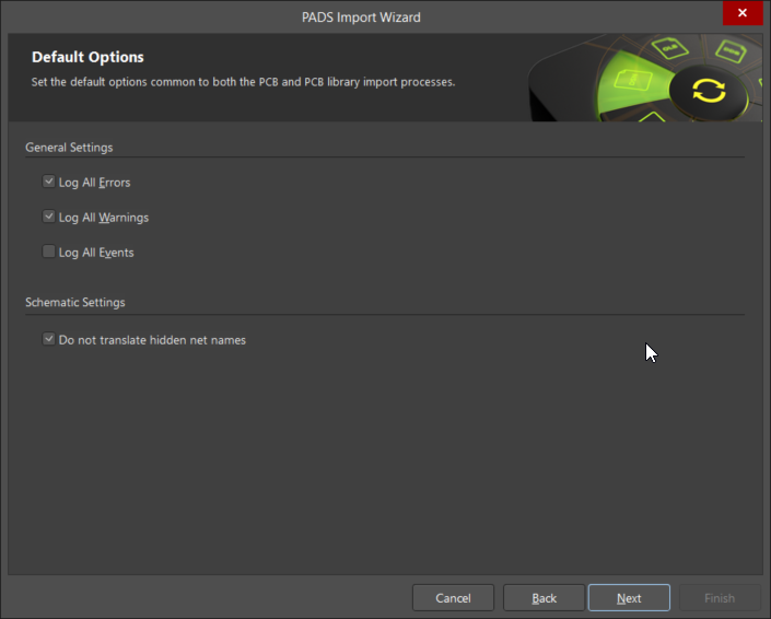
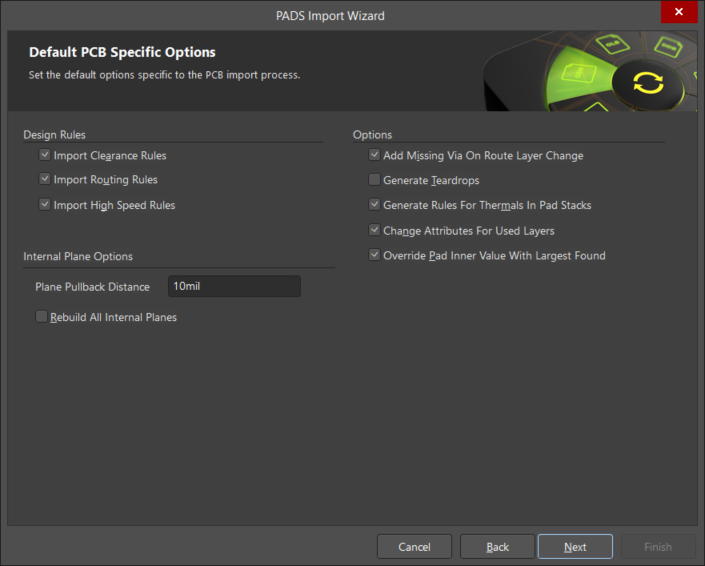
- The Import Wizard will now present several options for controlling the translation from PADS to Altium Designer Develop. You will be able to define which sets of design rules should be transferred, as well as how keep-outs are handled.
- If Generate Teardrops is enabled, the importer will add teardrops to all pads and vias in your design. If your design does not require teardrops, make sure to disable this option.
NOTE:
Altium Designer Develop will analyze PADS Split/Mixed layers to determine if the layer is being used as a mixed layer (i.e., has pour AND route data) or as a split plane layer (just pours). Mixed layers will be initialized as an Altium Plane (a negative layer) to take advantage of Altium’s split plane capabilities. If you wish the mixed layer to remain a positive image pour layer, remap the layer to one of Altium’s “Mid Layers” which are positive.
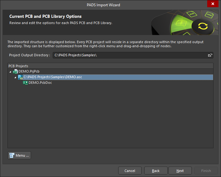
- You will now see a preview of the files that will be translated and their output directories. You can change the main output directory at this point if desired.
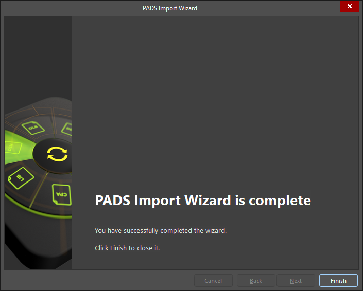
- Click the final Next button, and the Import Wizard will take care of the rest.
- Congratulations! Your design has been imported into Altium Designer Develop!
- Follow the Post Import Tidy Up checklist to ensure the design has been fully reviewed and verified.
- If you would like detailed information on how to carry out some of the tidy-up checks, please review our ‘Bringing Together Imported Schematic and PCB Designs’ guide.

Phase 4: Post Import Tidy Up
Once your migration is complete, we recommend checking your design to ensure that all data is transferred as expected. Below is a list of key checks to perform post-migration:
Physical check
- View » Fit Document
- Board shape and cutouts
Electrical check
- Netlist
Rules
- Have all rules been imported
- DRC check
- Check settings for polygons - Island removal, min primitive size
- Thermal reliefs, direct connect
- Check power plane settings
- Power plane Pull-back
- Solder mask, Paste mask rules
- Via Tenting
- Testpoint assignments
Power check
- Nets
- Planes
- Polygons
Documentation check
- Layers
- Text/Strings
- Legends
PCB reports
- Number of components/nets
- All nets routed
Getting Help
There are many ways to learn more about Altium Designer Develop:
- F1 over any object, editor, panel, menu entry, or button to open a brief description in your web browser
- Press Shift+F1 or ~ key while running a command for a list of shortcuts you can use in that command.
- Access our complete Altium Designer Develop Documentation online.
- Visit the Altium Video Library where you can watch training on over 150 different topics. Each video walks you through the steps needed to complete a task.
- All Altium Designer Develop subscription levels include easy access to real-time support, user communities, comprehensive product documentation, training videos, and knowledge base of targeted solutions for common user experiences. Contact Altium Support Here.
Additional Resources
Online Resources:
If you’re ready to dive deeper into the powerful features of Altium Designer Develop, below is a list of articles that
provide information to help you get started.
- For a full overview of the PCB design process with Altium Designer Develop, check out this tutorial: A Complete Design Walkthrough with Altium Designer Develop.
- For a look at the basics of creating components, read A Look at Creating Library Components.
- For a tutorial that steps you through all the basics of editing multiple objects, take a look at Schematic Placement and Editing Techniques in Altium Designer Develop.
- For an overview of How to Start an FPGA PCB Layout in Altium Develop Designer, read How to Start an FPGA PCB Layout For Your Embedded System.
Software Platform Resources:
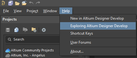
Another great way to get the most out of your Altium Designer Develop installation is by exploring its help section. You can launch the help menu on the left side of Altium Designer Develop by clicking Help and navigating to Exploring Altium Designer Develop.
Related Resources
Related Technical Documentation
Table of Contents
Design to Release, Without the Friction
- Keep reviews tied to the right version
- Reduce handoff confusion and rework
- Spot sourcing and release risk earlier
- Work solo, share when needed
Get Started
Thank you, you are now subscribed to updates.