


Planting Seeds in a Row SMT Component Placement Tolerance for your PCB


I had my 5-year-old nephew helping me spread flower seed this Spring. He got a kick out of throwing the seed out into the flower beds, but he didn’t pay attention to where he was throwing it. Most landed on the sidewalk. Before letting him continue, I decided to put some landscaping tape around the each bed’s perimeter. This helped the little guy get most of the seed into the right areas. With the flowers in order, we made sure to get a nice juice to cool us off.
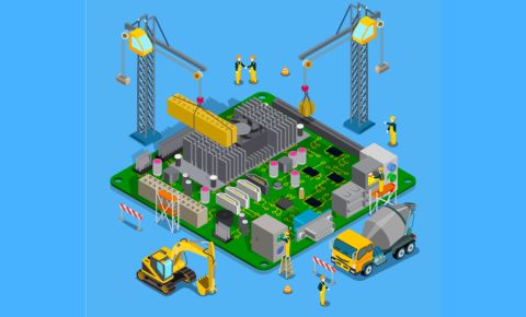
It got me thinking about printed circuit assemblies and the combination of design and manufacturing. That virtual parts and their placement courtyards become real hardware which machines accurately pick and place onto PCBs within microns of their defined locations. But unless the BOM software and PCB library accurately represents the hardware in a way that Purchasing could source, and factory machines know where to place, your design may wilt.
There are a few dimensions and their placement tolerances to keep in mind while designing your PCB. You want to define and bound the area where your component will be placed, and this will be determined from maximum tolerances for your component’s footprint and outline found on the datasheet. Your PCB Librarian will use these dimensions to establish the landing pattern and the courtyard for each component in your design.
Start with the PCB Footprint and Move to Your PCB Landing Pattern
A PCB starts with a Schematic containing components that the electrical engineer has selected for the design. Each component has dimensions found in its datasheet, including its IPC compliant characteristics. Most often, the component follows an IPC standard for its footprint, and you’ll use this to build its landing pattern.
The landing pattern is built using the component shape along with its footprint. The shape’s dimensions are given on the component datasheet, frequently in minimum, nominal, and maximum dimensions. To define the placement courtyard, the maximum dimensions of the shape will be used. This ensures enough tolerance is provided, so all components fit together on the PCB.
SMT Placement Courtyard Contains Component Shape and Landing Pattern
Using Maximum Tolerance for Fabrication Accuracy and Good Assembly
Now that you’ve defined the IPC compliant footprint maximums, along with the component shape maximums, you have your placement courtyard. This is the maximum area needed to accommodate all dimensions of the component and its landing pattern on the PCB. Knowing this, each component is assigned its unique place on the PCB using its placement courtyard.
And with each component having its unique placement on the PCB, the pick and place machines will be able to get the components into the right location during assembly. The SMT tolerance analysis includes fabrication details such as type of soldering and the mechanical keepouts needed for accurate assembly. The PCB producibility is achievable as tolerances have been used to define the SMT component placement courtyard, along with plating, etching, and registration to produce good assembly within the overall perimeter of the PCB.
Using Your PCB Design Software for Optimal PCB Layout
The next time you sit down to begin PCB layout with respect to SMT component placement tolerance, consider the amount and type of components you intend to use for your design. Using Active BOM can help you organize your design’s parts in one place. And then remind yourself of the mechanical sizing you’ve been allocated by the product team for your PCB. This will define the ultimate boundary within which you’ll need to sprinkle your SMT components.
Once you choose the SMT package size, you can use a PCB component wizard or any of your component management systems to build the placement courtyard for your SMT component. With each component having its designated space on the PCB, you are now ready to assign them their unique registration onto the PCB. This will ease placement accuracy with respect to each and every component in your design, facilitating accurate fabrication and assembly.
It is possible to clearly define where each and every SMT component will be placed within the perimeter of your PCB. Using the tools available within your PCB design software will help you visualize your landscape and keep you within the intended area of your project.
A PCB Component Wizard, or other component managers, will help your designs immensely.
When thinking about what PCB design software will work for you, I’ll always recommend keeping track of your design environment needs but also planning for the inevitable need to communicate with other members on your team. Thankfully, BOM tools can help bridge the communication gaps and ensure that there is no miscommunication.
Within the strong PCB design software that Altium provides, their ActiveBOM tool is available for real-time updating from schematic to layout to parts lists with consistent updating on part availability and component pricing changes. This will help your supply chain manage procurement of parts, so your competitors don’t grab them before you.
Knowing how to design for manufacturing is one part of the battle, the other part is having the software tools you need to design. If you’re curious about how to optimize your design process further with advanced BOM tools, talk to an expert at Altium today.
Related Resources
Related Technical Documentation
Table of Contents
Design to Release, Without the Friction
- Keep reviews tied to the right version
- Reduce handoff confusion and rework
- Spot sourcing and release risk earlier
- Work solo, share when needed
Get Started
Thank you, you are now subscribed to updates.