


Best Methods for Calculating SMD Pad Size in PCB Design

At a Glance
Component creation requires accurate SMD pad sizes in your PCB footprints. See how to determine pad sizes for your SMD components.


SMD components require precisely sized pads for soldering during assembly. PCB designers still have to create many of their footprints using information from data sheets along with general pad and land size formulas. The designer is responsible for ensuring pad sizes are correct, either by calculating them and comparing with footprint data, looking through datasheets, or by memorizing SMD pad size standards. If you have a component and you don't have access to the footprint, and you decide to biuld the footprint yourself, what resources are available to ensure you have the correct pad size?
Calculating SMD Pad Sizes
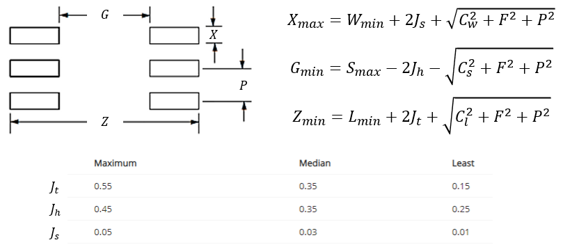
There are several ways to approach pad size determination for SMD components. The exact pad size determination will also depend on the type of component and the mounting style. For example, BGAs have different pad size requirement than leadless packages (like QFNs) and leaded packages (like SOIC or gullwing leads). As a general rule, pads are sized larger than the component lead with additional room for a solder fillet. These points are specified in the IPC-7351 standard as outlined below.
The IPC-7351B Standard
The IPC-7351B: Generic Requirements for Surface Mount Design and Land Pattern Standard provides requirements for land patterns for common components, which includes details on determining pad sizes. If you want to manually determine pad sizes, you can use the formulas outlined below to run these calculations for SMD components.
For more information on this standard and land pattern design, read this related article.
When in doubt about pad sizes for your components, check your datasheets! Component manufacturers provide all sorts of information in their datasheets, including physical package size and recommended land patterns. These land patterns will generally meet or exceed the spec in the IPC-7351B standard. For through-hole components, there is a separate standard, the IPC-7251: Generic Requirements for Through-Hole Design and Land Pattern Standard.
- For BGAs: The footprint for a BGA will also depend on the pitch in the package. Follow these guidelines to size pads in your BGA footprint. If you use solder-mask defined pads, make sure you account for slightly larger pad size so that the exposed pad area will be
The SMD Component Naming Convention in IPC-7351B
The IPC-7351B standard defines a naming convention for SMD components based on the component dimensions and land pattern. When searching component databases, the footprints for some IPC-standardized components will have a name that follows this convention. In this footprint naming convention, the first 3-7 characters are usually an acronym that defines the type of component package. The remaining information in the footprint name is then based on the lead information and body geometry. The naming convention follows the general pattern:
(Package type) + (Lead type) + (Lead pitch) + (Body length) + (Body width) + (Height)
If you are looking for components from online resources, or you find verified components from another library, this naming convention can help you decode the package information. The specific pad size required in these packages can be calculated with the methods listed above.
PCB Footprints Are More Than SMD Pad Sizes
The SMD pad size you use in your PCB footprint is important, but there are other aspects to include in a footprint to ensure the design can be successful successfully.
- Silk screen showing pin indicators, part outlines, and the location of a reference designator
- Assembly layer information to include in an PCB assembly drawing
- Solder mask opening with an expansion value applied in your PCB design rules
The solder mask opening layer and associated clearance rules are important for preventing DFA errors in the design and later defects during assembly. Your fabrication team and assembler can provide insight on these points to ensure your board is defect-free.
Your CAD Tools Might Include a PCB Footprint Calculator
The fastest way to method of creating footprints that I have found is to use the part building functionality that comes with your PCB layout tools. Many CAD systems today come with a footprint building tool that does the heavy lifting of part creation for you. Some of these tools also come with industry standard specifications already pre-loaded.
With these footprint builders as part of your PCB layout tools, you can save yourself a lot of time that you used to spend on creation. With the footprint specifications already loaded in the footprint builder, you can use it to build your according to the industry standards or make minor manual adjustments as needed. This will save you the time of having to research all of these specifications for yourself. The footprint builder also will create the for you with every pad and/or landing patterns, while adding necessary part outlines for silkscreen or assembly drawing shapes. This time your jaw might be dropping in wonder, not horror.
Every designer needs correct footprints inside their PCB design software, but no one likes creating them! When you use Altium, you'll have access to the IPC-compliant footprint wizard that will help you to create PCB footprints for your components. To help you manage your components, you can access the online library migration tools in Altium, where you can manage and share your design data.

About Author
Related Resources
Related Technical Documentation
Table of Contents
Design to Release, Without the Friction
- Keep reviews tied to the right version
- Reduce handoff confusion and rework
- Spot sourcing and release risk earlier
- Work solo, share when needed
Get Started
Thank you, you are now subscribed to updates.


