




The Right Way to Define PCB Trace Width

At a Glance
What seems like a simple selection of trace width is actually a critical engineering decision that relates to fabrication constraints and PCB stackup design.


Here we return to a fundamental engineering question in PCB design, and certainly one that may seem quite basic to the novice designer. That question is: how do we determine which trace widths to use in a particular stackup?
Simple designs built on 0.5 oz / 1 oz copper weight on inner/outer layers usually pick their trusty old 8 mil/0.2 mm trace width and get on with routing. Sometimes, these boards need a trace width adjustment for impedance control, but typically we can pick a trace width and stick with it.
In many other situations, such as designs with dense bottom-terminated parts, high layer counts, multiple impedance profiles, and heavier copper, we might find that the trusty old 8 mil/0.2 mm trace width no longer does the job. This article will look at all of the instances where we need to determine trace width constraints as driven by the stackup design and fabricator capabilities.
Always Start With the PCB Stackup
The PCB stackup is, literally and figuratively, the foundation for your circuit board design. Of course, it holds the components that can be assembled into the design, but it can also create constraints on what trace width is used to complete routing. The constraint on the trace width used in routing could come from multiple areas of the design and is the designer's responsibility to determine which of these are applicable to a particular layout or product.
In fact, what newer designers often don't understand is that the standard stackup found on most manufacturers' websites will not give you these constraints. Standard stackups are intended for simple designs where there are no hard constraints on trace width and clearances. It is often the case that real products require a designer to take ownership over stackup design and the associated constraint determination. If you find yourself in this boat, then pay attention to the areas below, which will help you constrain trace width and clearance to appropriate values.
Fabricator Capability and Copper Weight
The ultimate minimum trace width limit is imposed by your fabrication house capabilities, but this is not a single number you get from a website. An important point that many new designers don't realize, especially if they plan to work in power electronics, is that copper weight imposes a minimum trace width constraint. This is because heavier copper takes longer to etch, and narrower traces on thick copper may not be produced repeatedly over long etch times. Therefore, a fabrication house can only guarantee a certain minimum trace size as a function of copper weight.
Below is a table comparing typical trace width and clearance values from a fabrication house for three copper weight values and for internal and external layers.
0.5 oz/ft² Cu | 1.0 oz/ft² Cu | 2.0 oz/ft² Cu | |
Outer layers | 4.5 mil | 5.5 mil | 7.0 mil |
Inner layers | 3.5 mil | 4.5 mil | 6.0 mil |
You may have also noticed that the table separates trace width values into internal and external layers. One reason for this is that the internal layer copper does not require finished plating of through-holes and can have a smaller trace size and spacing allowance than the outer layers. Note that the copper weight values given here are finished copper weights, referring to the copper weight post-plating.
Fine-Pitch Bottom-Terminated Parts
While this category of parts includes large BGA packages, it is not limited to BGAs. Plenty of QFNs, LGAs, and even some leaded parts can have small pin pitch, which limits the trace width that should be used for routing into these components. This constraint can apply regardless of the required impedance value or copper weight.
Fine-pitch QFNs or LGAs can have pin pitch down to 0.5 mm, or 20 mil. At those pin pitches, you typically only get an 8 or 10 mil allowance for trace width at the high end. In other words, your trace width for routing into that component will be constrained at the low end by copper weight and at the high end by the physical size of the pads in the component footprint.
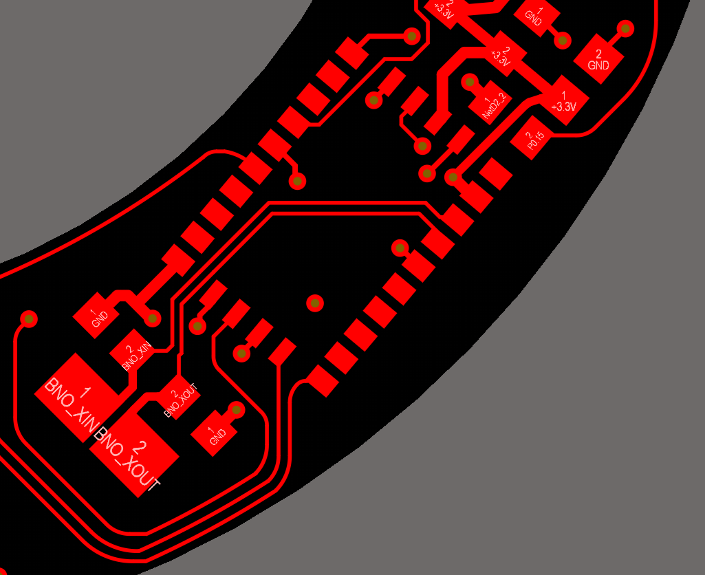
An important thing to understand about these parts is that the allowed trace width you can fit into the component pads will influence the stackup design when impedance control is required. For example, if you need to have a 10 mil wide microstrip at 50 ohms coming into a fine-pitch QFN package, the outer-layer dielectric cannot be thicker than approximately 5 mil.
BGA Footprints With High Pin Counts
BGA footprints may eliminate the ability to route between pins or pads, specifically when the pitch between the pins is small. These BGAs and the via fields used for fanouts can allow for routing between pads, but eventually ball pitch becomes so small that you cannot route between the vias or BGA pads without violating width and clearance limits. This sets an upper limit on the trace width that you can use, at least in the BGA region.
Most designers will take this trace width value and use it all over the board. This is partially for the convenience of setting up the design rules and constraints, and this way you are not required to create a neck-down rule as you route into the BGA footprint.

The other reason many designers will take this maximum trace width imposed by a BGA footprint and use it everywhere on the board is because it's highly likely there are other fine-pitch components on the board that can also benefit from the same trace width. This is another good reason to simply set a global preferred trace width in your design rules and just use it everywhere. Of course, there are exceptions, such as for controlled impedance or signal integrity, but these are often also addressed by selecting the right dielectric thicknesses in the PCB stackup.
Via Drill Hole Size Versus Trace Width
This constraint setup is much less common, but it is a useful way to prevent a drill breakout from a via pad from severing a connected trace. This is something you might do in a low-cost consumer product or in a throwaway device that does not need to achieve commercial or military reliability standards or workmanship.
Breakouts during drilling are shown in the image below. Depending on the IPC product class:
- Non-critical products can still allow breakout (Class 1)
- Breakout is limited (Class 2)
- Breakout is prohibited (Class 3)
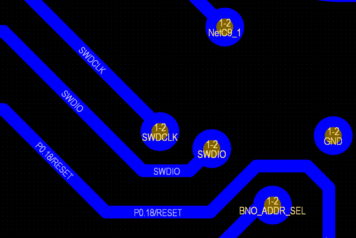
These 6 mil traces are connected to vias with 8 mil drill holes with sub-Class 2 annular rings, potentially leading to breakout. Increasing the trace width to 10 mil or adding tear drops will help ensure a trace does not detach when there is high drill wander.
From the image, it should be very clear to see that if the via pad is small, breakouts near the trace connection may completely sever the trace, and the PCB would need to be scrapped. However, as an alternative to using larger via pads, using a wider trace that is larger than the drill diameter will ensure that breakout does not fully sever the trace from the via pad.
Impedance Target
The final factor that determines a trace width constraint and is a direct consequence of the stackup design is the trace size needed for a target impedance. If you are using a standard stackup from a fabrication house, some stackups will give you the trace size for 50 ohm impedance, and then they will take a controlled impedance approach for differential pairs.
Altium Designer users can also get a highly accurate impedance calculation for single-ended traces or differential pairs using the impedance solver in the Layer Stack Manager. This is located on the Impedance tab and uses a built-in electromagnetic field solver engine to calculate the lossless impedance.

The Layer Stack Manager in Altium Designer includes a lossless impedance calculator.
This value can then be enforced as a design rule in your PcbDoc file during routing. Impedance values can be assigned to individual nets and net classes and can be enabled or disabled for specific layers.
Power Rail Sizing
Some of the instances listed above are all about finding and setting the maximum trace width, or finding a minimum trace width for routing small traces. But what about traces or rails for power electronics?
Power rails can be defined and set up using a design rule, just like standard traces, but they tend to require higher clearance and larger width than standard traces. These clearances and rail sizes depend on the voltage and current on the rail in question, and there is IPC guidance on sizing rails to prevent excessive IR drop on the power rail.
To size trace (or polygon) widths to prevent excessive voltage drop and keep rail temperature rise below a certain level, the IPC-2152 standard provides some guidance on the required cross-sectional area of a copper rail. This guidance is found in the tables below.
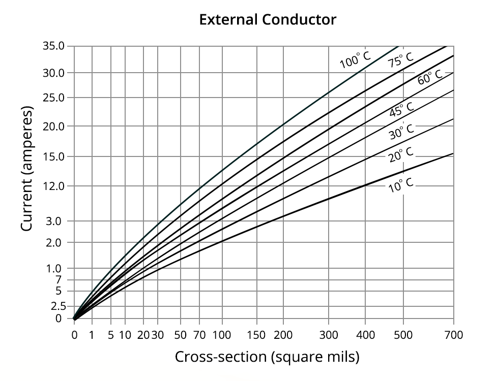
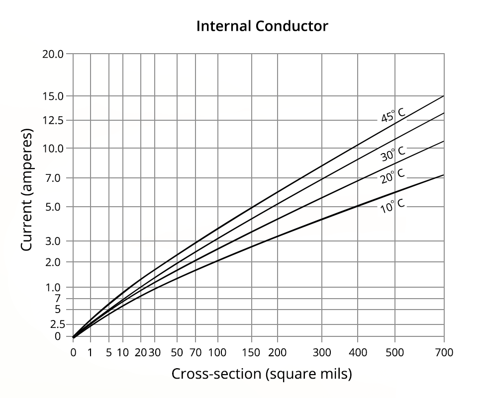
These tables show how the temperature rise limitation and current are related by the cross-sectional area: larger cross-section allows for higher current for a given allowed temperature rise. This makes sense as a larger cross section reduces current density, and therefore reduces the IR drop.
What about voltage and clearance? Clearance values only play a major role at high voltage and are addressed in a different standard (IPC-2221). The required clearance for a given DC/peak AC voltage can be calculated or determined from tabulated tables. We have also developed a calculator for this task which is found in another article:
Best PCB Routing Software for Enforcing PCB Trace Width Rules
If you want to ensure you maintain the right trace width throughout your design, including different values on different layers and in different regions of the PCB layout, you need PCB design software with a powerful and highly configurable PCB design rules engine. These trace width limits can be defined using a constraint matrix format or by setting limits for different categories of PCB design rules. However you prefer to set up your trace width constraints, Altium Designer's PCB design rules engine provides the capability and flexibility needed to control trace width everywhere in your design.
Trace Width Constraints by Layer
The PCB design rule system in Altium Designer allows users to create custom queries specifying where a design rule applies and to which objects it applies. To control traces on specific layers or groups of layers, you would use the OnLayer query to select traces on a specific layer. You can also create a group of layers, called a Layer Class, and use the InLayerClass query to call out traces on any layer in the group.

Classes can be created in Altium Designer so that design rules can be applied to groups of objects inside a class.
To define a trace width for a specific layer, create a Routing Width rule and use its scope query to select the required layer or layer class. This allows the minimum, preferred, and maximum trace widths to be enforced only where the corresponding query evaluates as true.
- Open the PCB Rules and Constraints Editor and locate the Routing - Width rule category.
- Create a new Width rule for the layer or group of layers that needs a unique trace width.
- Enter an OnLayer query for a single layer, such as OnLayer('Top Layer').
- For multiple related layers, create a Layer Class and use an InLayerClass query to scope the rule to that group.
- Enter the minimum, preferred, and maximum trace width values that should apply to the selected layers.
- Set the rule priority appropriately if another Width rule could also apply to the same routed objects.
- Route or modify traces normally, allowing Altium Designer to enforce the applicable width limits based on the active layer.
Trace Width Constraints by Region
Constraining trace width by region in the PCB layout is less common, but it is also possible with the query system inside Altium Designer. A Room object can define the physical area where a different width rule should apply, while the WithinRoom query identifies routed objects located inside that area.
- Create or place a Room around the portion of the PCB where the alternate trace width is required.
- Give the Room a clear name so that it can be referenced from the design rule query.
- Create a new rule under Routing - Width in the PCB Rules and Constraints Editor.
- Use a query such as WithinRoom('RoomName') to scope the Width rule to objects inside the specified Room.
- Enter the minimum, preferred, and maximum trace width values for that region.
- Adjust the rule priority if the regional rule overlaps with global, net-specific, or layer-specific Width rules.
- Route through the Room normally, allowing the regional Width rule to control the permitted trace dimensions.

Rooms can be defined in the PCB layout to establish regions where specific design rules apply.
Keep Trace Width Control Practical
PCB design rules simplify managing routing, manufacturing, and electrical constraints, eliminating the need to track exceptions manually. Rather than relying on rigid constraint systems or global settings, Altium Designer allows you to define rules based on actual PCB structures using custom queries. You can scope trace width constraints by net, layer, component, or physical region, maintaining a simple global rule while automatically enforcing high-priority exceptions where needed.
To learn more about the PCB design rules system in Altium Designer, watch the video below.
Whether you need to build reliable power electronics or advanced digital systems, use Altium’s complete set of PCB design features and world-class CAD tools. Altium provides the world’s premier electronic product development platform, complete with the industry’s best PCB design tools and cross-disciplinary collaboration features for advanced design teams. Contact an expert at Altium today!
Frequently Asked Questions
How does copper weight affect minimum PCB trace width?
Heavier copper generally requires a larger minimum trace width because thicker copper takes longer to etch. As etch time increases, very narrow traces become more difficult to manufacture consistently. Your PCB fabricator should therefore specify minimum trace width and spacing as a function of finished copper weight, rather than providing one minimum value for every layer.
How wide should a PCB power trace be for a given current?
PCB power trace width should be selected based on current, copper thickness, allowable temperature rise, and acceptable voltage drop. IPC-2152 provides guidance for determining the required copper cross-sectional area. Higher current or a lower allowable temperature rise generally requires a larger cross-section, which can be achieved with a wider trace, heavier copper, or both.
Can PCB trace width help prevent via drill breakout failures?
Yes. If drill wander causes breakout near the point where a trace connects to a via pad, a narrow trace can potentially be severed. Using a trace wider than the via drill diameter provides additional copper around the connection and reduces the chance that breakout will completely disconnect the trace. Teardrops can also provide additional copper at the via-to-trace transition.
How do I set different trace widths on different PCB layers in Altium Designer?
Create separate Routing - Width rules in the PCB Rules and Constraints Editor and scope each rule to the required layer. Use an OnLayer query for a single layer or create a Layer Class and use InLayerClass for multiple layers. Each rule can define its own minimum, preferred, and maximum trace widths, with rule priority determining which constraint applies when rules overlap.
How do BGA pitch and via size limit PCB trace width?
BGA pitch determines how much routing space is available between pads and fanout vias. As ball pitch decreases, the maximum trace width that can pass through the BGA region also decreases. At sufficiently small pitches, routing between pads or vias may no longer be possible without violating trace width and clearance limits, requiring narrower traces, smaller vias, or a different fanout strategy.

About Author
Related Resources
Related Technical Documentation
Table of Contents
- Always Start With the PCB Stackup
- Fabricator Capability and Copper Weight
- Fine-Pitch Bottom-Terminated Parts
- BGA Footprints With High Pin Counts
- Via Drill Hole Size Versus Trace Width
- Impedance Target
- Power Rail Sizing
- Best PCB Routing Software for Enforcing PCB Trace Width Rules
- Trace Width Constraints by Layer
- Trace Width Constraints by Region
- Keep Trace Width Control Practical
- Frequently Asked Questions
Solutions for Every Role and Team
- Discover and evaluate design options earlier
- Develop in one shared workspace
- Scale with control and compliance
- Connect every stage of hardware development
Learn More
Thank you, you are now subscribed to updates.



