


Best Tools For PCB DFM Checks

At a Glance
Sometimes, the best tool for PCB DFM checks is your PCB design software. Leverage your DRC engine to ensure compliance with DFM constraints.


Experienced designers know that DFM is not a checkbox on a PCB design review list. DFM is the grounding philosophy that drives what we do in PCB design. With a solid understanding of DFM constraints in the design, it's possible to avoid manufacturing defects and get the product right the first time.
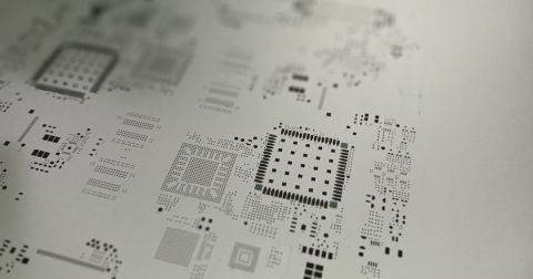
Executing DFM increasingly relies on software due to the complexity of PCB layouts. DFM constraints are imposed at multiple levels, starting from fabrication capabilities and being influenced by best industry practices and even certain quirks and component packages. The software used for DFM analysis should account for each of these constraint sets. We'll examine the options for DFM analysis tools in this guide.
Use the DRC Features in Your ECAD Software
The most effective tools anyone can use for DFM analysis are the automated DRC features in PCB design software. The key is knowing which DRCs to use and which values to set in the design rule definitions. PCB design rules can be defined both for electrical integrity purposes and manufacturability purposes, and it is the manufacturability side of design rule definition that ensures DFM constraints are properly enforced.
ECAD software allows two methods for defining PCB design rules which reflect DFM constraints:
- Category-based rules, which can be defined by layer, by net, or by net class
- Constraint matrix-based rules, where constraints are defined on an object-to-object basis
No matter how you choose to define PCB design constraints or rules, they should always be based on the capabilities of your manufacturer. PCB manufacturers publish their capabilities on their websites or provide them as PDF files upon request. If you have chosen a manufacturer, then make sure to get their capabilities so you can define your DFM constraints.
Category-Based DFM Rules
Design rules that enforce manufacturability are defined by assigning limits to objects in the layout based on their type or grouping. Clearance, width, hole size, and mask expansion values are entered once and applied to a defined scope, ensuring that traces, pads, and vias comply automatically as placement and routing progresses. These limits reflect fabrication tolerances such as minimum spacing, annular ring requirements, and solder mask registration.

These scoped rules can be applied across a broad range of categories, including clearance constraints, routing width constraints, hole size limits, solder mask expansion, paste mask reduction, polygon connect styles, and component placement spacing. Rules may be targeted to specific layers, net classes, differential pairs, component classes, or via types, allowing fabrication constraints to be embedded directly into the PCB data model.
Constraint-Based DFM Rules
An alternative approach defines manufacturability limits on an object-to-object basis using a structured constraint table. Instead of applying broad category limits, specific relationships between physical objects are defined numerically. This allows spacing, width, and geometry requirements to be tailored between particular nets, layer pairs, or component groupings without relying solely on class definitions.

Using this matrix-style configuration, designers can define copper clearance between different net classes, via span restrictions between layer pairs, differential pair gap limits, minimum solder mask sliver widths, backdrill constraints, and plane connection styles. Electrical, physical, and manufacturing constraints are centralized in a single structured view, making it easier to audit manufacturability requirements against a fabricator’s published capabilities.
Leverage Your Online and Batch DRCs
After DFM constraints are defined as outlined above, your ERC features in your CAD tools are your first line of defense against DFM violations. Online DRC checks design rule errors during placement and routing, immediately flagging them for correction while working on the PCB layout. Batch DRC checks are normally performed at or near the end of PCB layout in order to catch DFM and electrical violations which may not have been noticed during PCB layout. Leverage both processes with your DFM constraints to catch most of the simpler DFM errors in a PCB.
Post-Layout Tools For DFM Analysis
Once the PCB layout is complete, it will be exported to standard manufacturing outputs. When a PCB manufacturer wants to perform a DFM review on your design, they will not look at the native ECAD files. Instead, they look at the manufacturing outputs in a CAM software package. The PCB manufacturer will use this software to perform DFM analysis on the following files:
- Gerber files for copper and mask layers
- NC drill files for each layer span
- IPC-D-356 netlist
This is the minimum set of files needed to perform a DFM review prior to PCB fabrication. The CAM software will provide automated measurements of features in the Gerber layers.
HQDFM by NextPCB
NextPCB is a Chinese manufacturer providing fabrication and assembly services. They have also recently released a free piece of software called HQDFM. The software is free to download and use on your local machine and can be used to examine design outputs before fabrication. It also automates some basic DFM checks on your manufacturing output files. Users can then quickly place their design into production with NextPCB.

HQDFM software [Source: NextPCB]
As is the case with any overseas manufacturer, be mindful of export control regulations and IP concerns. While the HQDFM platform runs on Amazon Web Services, one should be careful with overseas services, as you never know who might be getting a peek at your design data.
Numerical Innovations FAB 3000
Numerical Innovations develops some of the leading-edge CAM software used in the industry, with their flagship product being FAB 3000. This CAM software automates many aspects of the analysis on manufacturing outputs and provides an error report for users. Errors are flagged based on custom design rules which are set to match the manufacturer's capability.

CAMtastic! Viewer in Altium Designer
Altium Designer is the only PCB design application that includes an integrated CAM environment as part of the standard installation. When generating manufacturing outputs, it is advisable to automatically create a CAM document alongside Gerber, drill, or IPC outputs. This enables direct inspection of fabrication data inside the same software environment used for layout.

With the CAM environment loaded, designers can compare copper features, drill hits, solder mask openings, and net connectivity against the original layout. This reduces ambiguity between design intent and exported data and allows early detection of issues such as missing apertures, incorrect polarity, drill span mismatches, or netlist discrepancies before files are released to fabrication.
IPC-2581 Viewers
For users of the IPC-2581 smart data format, there are multiple viewer products that are endorsed by the IPC-2581 Consortium and can be run on your desktop computer. Users can apply the same type of analysis to IPC-2581 archives that they would use on other design output formats. As a smart data format, IPC-2581 archives can also be examined in other ways beyond DFM, such as reviewing the BOM, placement, footprints, and many other factors as would be seen by a manufacturer.
DFM Always Starts in the PCB Layout
No matter which DFM tool you use, DFM always starts in the PCB layout inside your ECAD software. Design rules and constraints are the absolute best tool for preventing DFM errors before completing a PCB layout. Anytime there are DFM errors at the completion of a layout, the PCB will need to be modified, which ultimately takes time and incurs extra cost.
Whether you need to build reliable power electronics or advanced digital systems, use Altium’s complete set of PCB design features and world-class CAD tools. Altium provides the world’s premier electronic product development platform, complete with the industry’s best PCB design tools and cross-disciplinary collaboration features for advanced design teams. Contact an expert at Altium today!
Frequently Asked Questions
What is design for manufacturing?
Design for manufacturing (DFM) refers to allowing manufacturing constraints to define what is allowed in a PCB design. It requires that the designer understand the fabrication and assembly limitations of their vendors, and then implement those limitations as design rules.
Can PCB design software replace standalone DFM tools?
No, but the reverse is also true: DFM tools cannot replace the design rules found in PCB design software. Smart designers leverage both their design rules and CAM software to fully evaluate conformance to DFM requirements.
Are Gerber files sufficient for a complete DFM analysis?
Gerber files alone are not sufficient for a full DFM analysis. When examining manufacturing outputs, the DFM tool should also look at the CNC data in the drill file for each layer span used in the design. When the design is reviewed by a manufacturer, they will also need the fabrication notes and assembly notes to ensure they are imposing the correct DFM constraints in their review.
When should DFM checks be performed during the PCB design process?
PCB design software with online DRC capabilities will check certain design rules in real time as the PCB layout is being completed. This means any design rules that are defined based on DFM constraints can automatically be checked during layout. Once the layout is completed, CAM software and a manufacturer’s review should be performed in order to identify any outstanding DFM problems.
What is the difference between category-based and constraint-matrix DFM rules?
The primary difference is in the user interface. Matrix-based DFM rules are used in some older PCB design software, and so they continue to be used as it is preferred by some designers. A category-based approach is more modern but still provides the same capability as a matrix approach.
About Author
Related Resources
Related Technical Documentation
Table of Contents
- Use the DRC Features in Your ECAD Software
- Category-Based DFM Rules
- Constraint-Based DFM Rules
- Leverage Your Online and Batch DRCs
- Post-Layout Tools For DFM Analysis
- HQDFM by NextPCB
- Numerical Innovations FAB 3000
- CAMtastic! Viewer in Altium Designer
- IPC-2581 Viewers
- DFM Always Starts in the PCB Layout
- Frequently Asked Questions
Design to Release, Without the Friction
- Keep reviews tied to the right version
- Reduce handoff confusion and rework
- Spot sourcing and release risk earlier
- Work solo, share when needed
Get Started
Thank you, you are now subscribed to updates.

