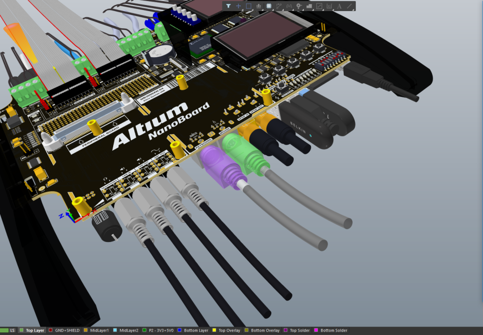
Mobile menu
  • Discover
  • Develop
  • Agile
  • Resources & Support
    Free Altium 365 Tools
    • Gerber Compare
    • Online PCB Viewer
    Resources & Support
    • Learning Hub
    • Support Center
    • Documentation
    • Webinars
    Altium Community
    • Forum
    • Bug Crunch
    • Ideas
  • Education
    • Student Lab
    • Educator Center
    • Altium Education Curriculum
  • Search Open
    Search Close
Sign In
PCB Layout

Main menu

  • Home
  • PCB Design
    • Collaboration
    • Component Creation
    • Data Management
    • Design Outputs
    • ECAD/MCAD
    • HDI Design
    • High Speed Design
    • Multi-Board
    • PCB Layout
    • PCB Routing
    • PCB Supply Chain
    • Power Integrity
    • RF Design
    • Rigid Flex
    • Schematic Capture
    • Signal Integrity
    • Simulation
  • Software
    • Develop
    • Discover
    • Agile
    • Altium 365
    • Altium Designer
  • Education
    • Programs
    • Altium Academy
    • Engineering News
    • Guide Books
    • Newsletters
    • Podcasts
    • Projects
    • Training Courses
    • Webinars
    • Whitepapers
Learning Hub PCB Layout

PCB Layout

A high-quality PCB layout involves component placement that allows tight routing, ensures low EMI, and satisfies mechanical constraints. Browse our library of resources to learn strategies for successful PCB layout.

How to Create a PCB Layout from a Schematic Route Your Most Complex Boards Faster PCB Design and Development Top 5 PCB Design Rules Board Layout with Altium PCB Layout and Placement Guidelines PCB Component Placement (Webinar) Rules-Based Component Placement Altium Develop PCB Layout Capabilities Design Rules Available for PCB Layout in Altium
  • Overview
  • All Content
  • Webinars
Filter
found
Sort by
Role
Software
Content Type
Region
Clear Filters
pcb layout guidelines Top 5 PCB Design Layout Guidelines You Need to Know 14 min Blog PCB Design Engineers Manufacturing Engineers PCB Design Engineers PCB Design Engineers Manufacturing Engineers Manufacturing Engineers We've compiled some of the essential PCB layout guidelines every designer should know to ensure your board will work as intended. Written by a leading industry expert. Read Article
Group Components into Rooms for More Efficient Layout Group Components into Rooms for More Efficient Layout 4 min Whitepapers The key to properly managing your component placements and traces is to utilize different techniques of grouping objects together rather Read Article
44 How to Edit Copper Polygons on your PCB Layout on Altium Designer 17 PCB Design Software 1 min Videos Read Article

Pagination

  • First page « First
  • Previous page ‹‹
  • Page54
  • Page55
  • Page56
  • Page57
  • Page58
  • Current page59
Platform-based Solutions
  • Discover
  • Develop
  • Agile
Tools
  • Altium Designer
  • Octopart
Platform
  • Altium 365
Product Extension
  • Power Analyzer
  • Signal Analyzer
Company
  • Our Customers
  • Trust Center
  • Newsroom
Resources & Support
  • Status
  • Downloads
  • Learning Hub
  • Support Center
  • Bug Crunch
  • Forum
  • Documentation
  • Ideas
  • Education
  • Professional Training / Certification
  • Webinars
  • Beta Program
Education
  • Student Lab
  • Educator Center
  • Altium Education Curriculum
Careers
  • Career at Altium
  • Copyrights & Trademark
  • Privacy policy
  • Cookie policy
  • Terms of Service
  • Legal
© 2026 Altium Pty. Ltd.