


Conductive Ink Printing for PCB Designers: What You Need To Know

At a Glance
Explore how conductive ink printing enables rapid PCB prototyping on flexible and 3D surfaces—plus design tips, DFM rules, and alternatives for PCB designers.


Rapid prototyping has long been a challenge in the electronics industry. While traditional PCB manufacturing methods involve multi-day processes and fixed-form factors, innovations in conductive ink printing have expanded the range of design options for PCB designers. This technology continues to evolve as a viable method for fast-turn design and production, particularly when printed onto flexible or unconventional substrates.
Conductive ink printing is also compatible in some 3D printing processes and equipment for unconventional surfaces, including curved surfaces or angled surfaces. At industrial scales, 3D printing has seen increased adoption which can enable conductive ink-based PCB designs to move from prototyping or one-off designs into a volume production opportunity. Furthermore, 3D printer manufacturers are revolutionizing rapid PCB prototyping by introducing advanced features that were previously impossible, like printing multilayer PCBs.
What Is Conductive Ink Printing and How Does It Work in PCBs?
Conductive inks are suspensions of metal nanoparticles and a liquid that can be deposited onto various insulating substrate materials, including PCB substrates. Conductive materials used in these inks include copper, silver, or gold. Conductive ink printing allows PCBs to be fabricated in an additive process, where the conductor is deposited directly on a dielectric, or the dielectric is also deposited in its own printing process. This is very different from the conventional method of PCB manufacturing, in which copper layers are etched away in a subtractive process.
3D printers are the primary tools used to apply conductive inks in order to form a conductive layer for circuits and traces. This has lead to a handful of 3D printer companies developing specialized 3D printers for PCB prototyping, such as Nano Dimension. Due to the throughput of 3D printing processes, even at industrial scale, conductive ink printed designs are possible at lower volume and/or high part mix.

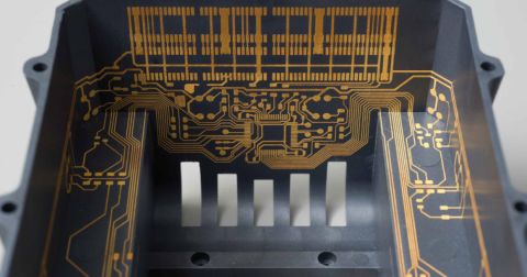
3D-printed conductive inks can be compatible with a variety of substrate materials, including curved or flexible substrates
3D printing processes for depositing conductive inks include three common options:
- Aerosol jetting, where a suspension is aerosolized and deposited towards a substrate at high velocity
- Inkjet printing, where a suspension is dropped on a substrate directly
- Stereolithography, where an ink is cured in place after exposure to a laser image of the conductive pattern
- Fused deposition molding, where a thick conductive paste is deposited and sintered to form traces
These processes are commercially available for use with flat and curved surfaces at low volume/high mix. Their usage falls into rapid prototyping and production, typically providing a completed PCB within hours, depending on the size and complexity of the circuit. In some cases, substrate co-deposition is also available with unique dielectric insulating materials, which can then be put into reflow soldering for PCB assembly.
One of the common applications of conductive printing on 3D surfaces or on curves is in RF design. For example, this allows the printing of unique antenna designs or antenna arrays and their associated RF-printed circuits. Using curved surfaces allows unique antenna designs and arrays to exploit functionality that would be very difficult on flat surfaces, such as very large scan angles in beamformer antenna arrays. These 3D surfaces can be built with unique material sets that have a range of Dk values, overall giving more control over unique antenna functions.
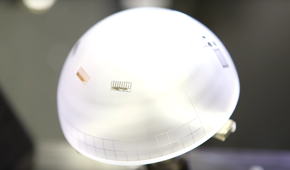
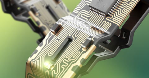
Conductive structures printed on a hemispherical surface with an Optomec five-axis aerosol jet 3D printer.
DFM Rules For Conductive Ink Printing
As is the case in any PCB design, there are manufacturing constraints, which are DFM rules for the PCB designer. Conductive ink printing capabilities are comparable to advanced etching processes (e.g., laser direct imaging) as long as the right deposition process is used. Still, PCB designers need to have some limitations imposed on the copper trace geometries used in a 3D printed part:
- Trace width limitation
- Etch factor
- Trace thickness limitations on flat surfaces
- Allowed hole diameter for via formation (if applicable)
- Allowed trace thickness limitation on curved surfaces
The resulting smoothness of the deposited ink becomes important in the case of high-speed designs requiring controlled impedance, and the roughness profile can be very different in comparison to controlled impedance designs. Conductive ink printing rules and the profilometry results for deposited copper can vary greatly by material composition, printing process, and printing equipment, all of which are not standardized. If you plan to pursue conductive ink printing as a fabrication process, consult your printing equipment vendor or work with your fabricator to build test coupons for full characterization.
Alternatives to Conductive Ink Printing
Conductive ink printing is widely used as a direct deposition solution for commercial printed circuit boards, but this is typically done on a planar substrate or during co-deposition of the insulating substrate material. Conductive inks, insulating dielectric inks, and insulating substrates offer a broad range of design approaches and material pairings that can enable many unique devices and applications. However, there are alternative approaches to fabricating conductive traces on 3D surfaces, including curved surfaces.
One of these processes is laser direct structuring, which can be used with injection-molded parts made from thermoplastic materials. A laser-direct structuring process follows these steps:
- The deposition surface is first activated with a laser in preparation for the deposition
- The activated areas are plated with copper using an electroless process
- The electroless copper is finished by applying a standard surface plating
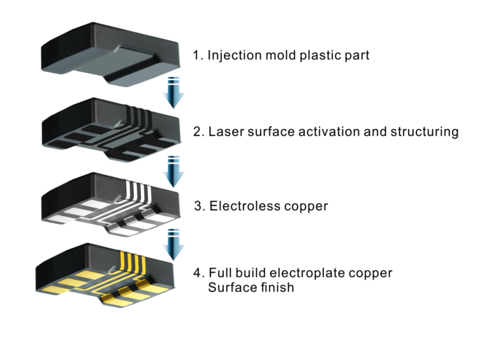
Process image courtesy of Unictron Technologies Corp.
By eliminating the conductive ink and instead relying on electroless plating, fabrication now relies on a much more familiar process without the need for new capital equipment. Electroless plating also enables high-density designs as it enables very high resolution, something that is not possible with all conductive ink processes.
To learn more about 3D PCB designs on curved insulating surfaces, watch our recent podcast episode with Jack Henriques, Altium Product Manager.
Have more questions on conductive ink printing with 3D printers? Talk to an expert at Altium.
Whether you need to build reliable power electronics or advanced digital systems, use the complete set of PCB design features and world-class CAD tools in Altium. To implement collaboration in today’s cross-disciplinary environment, innovative companies are using Altium to easily share design data and put projects into manufacturing.

About Author
Related Resources
Table of Contents
Design to Release, Without the Friction
- Keep reviews tied to the right version
- Reduce handoff confusion and rework
- Spot sourcing and release risk earlier
- Work solo, share when needed
Get Started
Thank you, you are now subscribed to updates.


