Mobile menu
  • PCB Design
    • Altium Designer World’s Most Popular PCB Design Software
    • CircuitStudio Entry Level, Professional PCB Design Tool
    • CircuitMaker Free PCB design for makers, open source and non-profits
    • Why Switch to Altium See why and how to switch to Altium from other PCB design tools
  • Solutions
    • For Enterprise The Last Mile of Digital Transformation
    • For Parts and Data Extensive, Easy-to-Use Search Engine for Electronic Parts
  • Altium 365
  • Resources & Support
    Explore Products
    • Free Trials
    • Downloads
    • Extensions
    Free Altium 365 Tools
    • Online PCB Viewer
    Resources & Support
    • Renesas / Altium CEO Letter To Customers
    • Learning Hub
    • Support Center
    • Documentation
    • Webinars
    Altium Community
    • Forum
    • Bug Crunch
    • Ideas
  • Training & Education
    Professional Training
    • Courses & Certificates
    • Training Previews
    • On-Demand
    • Instructor-Led Trainings
    Education
    • Programs
    • Educator Center
    • Student Lab
    • Altium Education Curriculum
  • Store
  • Search Open
    Search Close
Sign In
Videos

Main menu

  • Home
  • PCB Design
    • Collaboration
    • Component Creation
    • Data Management
    • Design Outputs
    • ECAD/MCAD
    • HDI Design
    • High Speed Design
    • Multi-Board
    • PCB Layout
    • PCB Routing
    • PCB Supply Chain
    • Power Integrity
    • RF Design
    • Rigid Flex
    • Schematic Capture
    • Signal Integrity
    • Simulation
  • Software
    • Altium 365
    • Altium Designer
    • Enterprise Solutions
    • PDN Analyzer
    • Upverter
  • Education
    • Programs
    • Altium Academy
    • Engineering News
    • Guide Books
    • Newsletters
    • Podcasts
    • Projects
    • Training Courses
    • Webinars
    • Whitepapers
  • FREE TRIALS
Learning Hub Videos Harness Design Demonstration

Harness Design Demonstration

Harness design

Registration has recently closed. Check back soon for on-demand webinar.

Related Resources

47:55 ECAD-MCAD CoDesign with Altium 365 & SOLIDWORKS MCAD CoDesigner allows for seamless collaboration between electrical and mechanical domains and has the exact fit and form factor of Watch Video
15:20 ON Demand - XJTAG Watch Video
1:04 DRC Flexibility - Features Watch Video
1:52 How To Quickly Create a Title Block in Draftsman Watch Video

Related Technical Documentation

Adding Via Stitching & Via Shielding to a PCB in Altium Designer Adding Via Stitching & Via Shielding to a PCB in Altium Designer

This page looks at the PCB Editor's support for via stitching (used to tie together larger copper areas on different layers) and via shielding (used to help reduce crosstalk and electromagnetic interference in a route that is carrying an RF signal)

Read Documentation
Updating Footprints from Libraries in Altium Designer Updating Footprints from Libraries in Altium Designer

Explore Altium Designer 24 technical documentation for Updating Footprints from Libraries and related features.

Read Documentation
Measuring Distances on a PCB Document in Altium Designer Measuring Distances on a PCB Document in Altium Designer

Explore Altium Designer 24 technical documentation for Measuring Distances on a PCB and related features.

Read Documentation
Preparing a PCB for Routing in Altium Designer Preparing a PCB for Routing in Altium Designer

Explore Altium Designer 24 technical documentation for Preparing a PCB for Routing and related features.

Read Documentation
Replicating PCB Layout for a Flat Design in Altium Designer Replicating PCB Layout for a Flat Design in Altium Designer

Explore Altium Designer 24 technical documentation for PCB Layout Replication and related features.

Read Documentation
Designing a PCB with Embedded Components in Altium Designer Designing a PCB with Embedded Components in Altium Designer

This page looks at the PCB Editor's support for embedded components - components that are manufactured as discrete entities and then placed on an inner layer of the circuit board during fabrication/assembly

Read Documentation
Defining High Speed Signal Paths with xSignals in Altium Designer Defining High Speed Signal Paths with xSignals in Altium Designer

This page looks at the xSignals feature, which enables the correct treatment of a high-speed signal path as just that - a path for a signal to travel between a source and destination, through termination components as well as branches

Read Documentation
Release Notes for PDN Analyzer Release Notes for PDN Analyzer

This page presents a full listing of the release notes for each public release of PDN Analyzer

Read Documentation
Controlled Depth Drilling (Back Drilling) in Altium Designer Controlled Depth Drilling (Back Drilling) in Altium Designer

This page takes a detailed look at Controlled Depth Drilling (CDD), also known as back drilling - a technique used to remove the unused portion, or stub, of copper barrel from a thru-hole in a printed circuit board

Read Documentation
Modifying Existing Routes on Your PCB in Altium Designer Modifying Existing Routes on Your PCB in Altium Designer

Explore Altium Designer 24 technical documentation for Modifying Existing Routes and related features.

Read Documentation

Harness Design Demonstration

Created: February 20, 2024
1 video
  • 00:58:10 • Feb 19, 2024
    00:58:10 • Feb 19, 2024
Product: Altium Designer Videos Webinars PCB Design Engineers Multi-Board Harness Design System and Product-Level Design

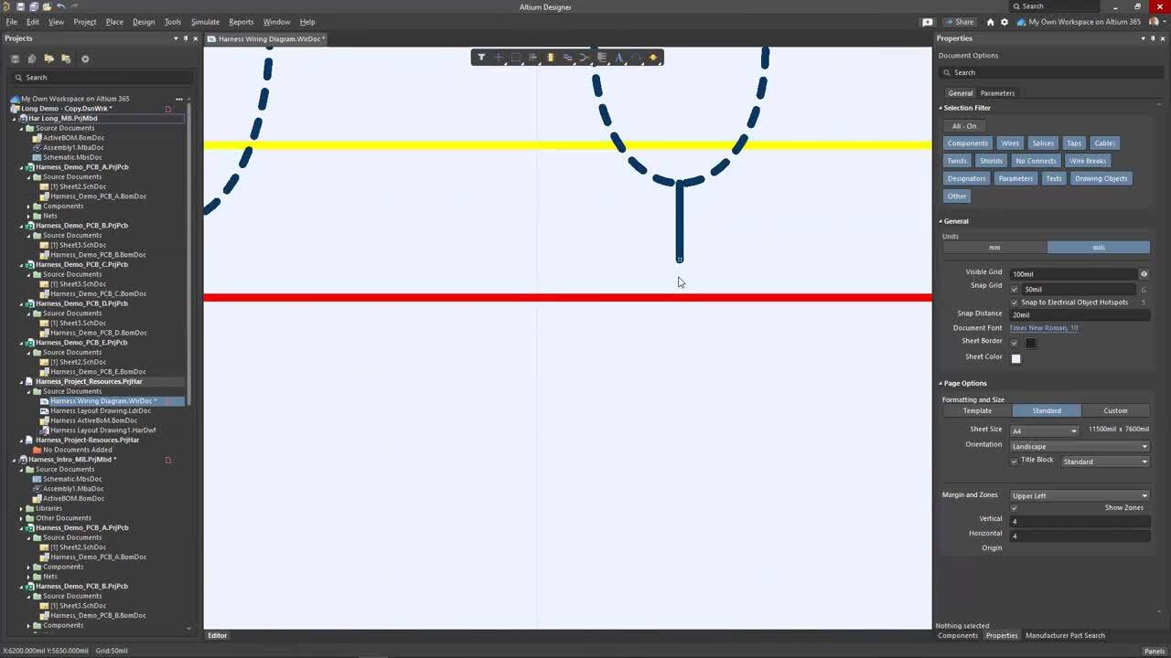
This video demonstrates the full range of cable harness design features integrated in Altium, including newly enhanced capabilities that surpass conventional third-party tools. We'll guide your step-by-step through a dedicated harness project integrated within a larger multiboard project, illustrating how to synchronize the schematic wiring document with the Multiboard schematic via an Engineering Change Order.

You’ll learn how to create new harness components within Altium and then place them from the library. We’ll also show you how to manage multiple harnesses efficiently in a single multiboard project.

All project files featured in this demonstration are included in your set of Altium's example projects in:

C:\Users\Public\Documents\Altium\AD<version>\Examples\HarnessDemo MB\Harness_Demo_Prj folder

Additionally, two supporting libraries are being used which can be downloaded here.

Related Resources

47:55 ECAD-MCAD CoDesign with Altium 365 & SOLIDWORKS MCAD CoDesigner allows for seamless collaboration between electrical and mechanical domains and has the exact fit and form factor of Watch Video
15:20 ON Demand - XJTAG Watch Video
1:04 DRC Flexibility - Features Watch Video
1:52 How To Quickly Create a Title Block in Draftsman Watch Video

Related Technical Documentation

Adding Via Stitching & Via Shielding to a PCB in Altium Designer Adding Via Stitching & Via Shielding to a PCB in Altium Designer

This page looks at the PCB Editor's support for via stitching (used to tie together larger copper areas on different layers) and via shielding (used to help reduce crosstalk and electromagnetic interference in a route that is carrying an RF signal)

Read Documentation
Updating Footprints from Libraries in Altium Designer Updating Footprints from Libraries in Altium Designer

Explore Altium Designer 24 technical documentation for Updating Footprints from Libraries and related features.

Read Documentation
Measuring Distances on a PCB Document in Altium Designer Measuring Distances on a PCB Document in Altium Designer

Explore Altium Designer 24 technical documentation for Measuring Distances on a PCB and related features.

Read Documentation
Preparing a PCB for Routing in Altium Designer Preparing a PCB for Routing in Altium Designer

Explore Altium Designer 24 technical documentation for Preparing a PCB for Routing and related features.

Read Documentation
Replicating PCB Layout for a Flat Design in Altium Designer Replicating PCB Layout for a Flat Design in Altium Designer

Explore Altium Designer 24 technical documentation for PCB Layout Replication and related features.

Read Documentation
Designing a PCB with Embedded Components in Altium Designer Designing a PCB with Embedded Components in Altium Designer

This page looks at the PCB Editor's support for embedded components - components that are manufactured as discrete entities and then placed on an inner layer of the circuit board during fabrication/assembly

Read Documentation
Defining High Speed Signal Paths with xSignals in Altium Designer Defining High Speed Signal Paths with xSignals in Altium Designer

This page looks at the xSignals feature, which enables the correct treatment of a high-speed signal path as just that - a path for a signal to travel between a source and destination, through termination components as well as branches

Read Documentation
Release Notes for PDN Analyzer Release Notes for PDN Analyzer

This page presents a full listing of the release notes for each public release of PDN Analyzer

Read Documentation
Controlled Depth Drilling (Back Drilling) in Altium Designer Controlled Depth Drilling (Back Drilling) in Altium Designer

This page takes a detailed look at Controlled Depth Drilling (CDD), also known as back drilling - a technique used to remove the unused portion, or stub, of copper barrel from a thru-hole in a printed circuit board

Read Documentation
Modifying Existing Routes on Your PCB in Altium Designer Modifying Existing Routes on Your PCB in Altium Designer

Explore Altium Designer 24 technical documentation for Modifying Existing Routes and related features.

Read Documentation
Back to Home
Altium Designer Logo

Take advantage of the world's
most trusted PCB design system.

One interface. One data
model. Endless possibilities.

Effortlessly collaborate with
mechanical designers.

The world's most trusted
PCB design platform

Best in class interactive
routing

View License Options

Try Altium Designer
Which best describes you?
Step 1 of 2
Try Altium Designer
Which best describes you?
I’m a Professional
I’m a Student University Email Required
I’m a Startup
Back
Step 1 of 2
Back
Step 1 of 2
PCB Design
  • Altium Designer
  • CircuitStudio
  • CircuitMaker
  • Altium 365 Viewer
How to Buy
  • Store
  • Regional Resellers
  • Special Offers
Solutions
  • For Enterprise
  • For Parts and Data
  • Altium 365
Contact Us
Product Extension
  • All Extensions
  • Power Analyzer
  • Signal Analyzer
Company
  • About Altium
  • Our Customers
  • Corporate Governance
  • Trust Center
  • Hire an Expert
  • Partners & Alliances
  • Partner Job Openings
  • Newsroom
  • Affiliate Program
  • Launchpad Startup Program
Resources & Support
  • Free Trials
  • Status
  • Downloads
  • Learning Hub
  • Support Center
  • Bug Crunch
  • Forum
  • Documentation
  • Ideas
  • Education
  • Professional Training / Certification
  • Secondary / High School
  • University / College
  • Webinars
  • Beta Program
PCB Design Guides
  • Component Creation and Management
  • High-Speed PCB Design
  • PCB Layout
  • PCB Routing
  • Schematic Capture and Schematic Entry
  • PCB Design Collaboration
  • ECAD/MCAD PCB Design
  • Multi-Board PCB Design
Careers
  • Career at Altium
  • Copyrights & Trademark
  • Privacy policy
  • Cookie policy
  • Terms of Service
  • End-User License Agreement
  • Legal Notice
© 2025 Altium Pty. Ltd.