


Transmission Line Impedance Calculation With Altium Designer

At a Glance
Today’s PCBs contain many transmission lines. Combine this with increased clock frequencies and data rates and the result is a critical challenge to high-speed design. Neglecting these dynamics can undermine product development by compromising performance, power consumption, EMC/EMI compliance, and more - leading to delayed design cycles and opening gaps that can be exploited by your competition.
Hone your high-speed design skills by joining us as we discuss the typical transmission lines encountered in today’s designs, the PCB variables that affect impedance, as well as how to create, calculate, and design transmission lines in Altium Designer. Learn how to maximize the built in SIMBEOR® engine by Simberian to craft impedance profiles and manage transmission lines in your designs.
This Live Webinar recording covers the following:
Current trends in electronics development
PCB transmission line model and impedance calculations
Transmission line with specified impedance in Altium Designer
Don’t pass up on this opportunity to experience the industry’s best in class design experience!


Editor's note: While originally presented for Altium Designer 20, the features shown here are applicable in later versions of Altium Designer. The design workflow and configuration of design rules has not changed. For more information on these features in the newest version of Altium Designer, read the documentation.
Introduction
Many of today's PCBs run with high-speed signals, so many traces in a typical board will act like transmission lines. Combine this with increased clock frequencies and data rates and the result is a critical challenge to high speed design. Neglecting these dynamics can undermine product development by compromising performance, power consumption, EMC/EMI compliance, and more - leading to delayed design cycles and opening gaps that can be exploited by your competition.
Hone your high-speed design skills by joining us as we discuss the typical transmission lines encountered in today’s designs, the PCB variables that affect impedance, and how to create, calculate, and design transmission lines in Altium Designer. You'll learn how to maximize the built-in SIMBEOR® engine by Simberian to craft impedance profiles for transmission lines in your designs. We'll start with the standard model for a transmission line impedance calculation and show how to enable impedance calculations as design rules for the interactive routing features in Altium Designer.
Impedance Profiles
We're going to start by talking about current electronics development trends. Introducing a simple concept of the transmission line model and how impedance on these transmission lines are either intentionally or inadvertently manifested on printed circuit boards. We're going to follow that with a discussion on a very important topic called Return Current. Then we're going to review the PCB design, some of the key PCB design rules, and how they influence impedance.
Current Electronics Development Trends
Everyone knows that everything's going faster every year and we're expected to do it in a quicker amount of time, using a smaller footprint, and lower power consumption. A great example is Ethernet data rates that have been increasing dramatically, all the way up to 100 gigabits and beyond these days. At the same time, we see an increase in clock rates. These increases result in reduced edges of the signal and quicker rise and fall times.
Data transfer rate over Ethernet by year
Transmission Line Impedance Model
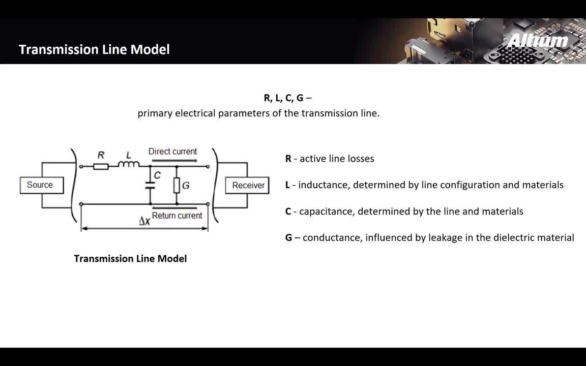
A transmission line is formed by a pair of conductors which carry a propagating current waveform. The current carried on the transmission line generates an electric field and magnetic field. Examples of transmission lines are the cable you use for satellite or terrestrial base cable TV. All conductors have some resistance (R), but this is not the only factor that determines impedance. Because the two conductors that form the transmission line make a closed loop, the line has some inductance (L). Next, when we look at a drawing here representing the spacing between the signal line and its return path, the two sections of the line are separated by a dielectric, which creates some capacitance (C). Finally, the dielectric between the two sections of conductor has its own DC conductance and losses (G), which reduces the energy carried by the signal on the transmission line. These are the main factors that influence transmission line performance.
When we talk about transmission line impedance in a circuit board, we often see microstrips with the conductor on the top layer and a return plane on an adjacent layer separated by the dielectric substrate. In the above circuit diagram, the R, L, C, and G values are not real circuit elements, they are distributed along the length of the transmission line. These terms are per unit length values, so we use a distributed circuit model to describe how a signal propagates along a transmission line. As a signal propagates, the return current is induced along the line into the return plane as a displacement current. This is shown schematically below.
When you have an impedance mismatch at each end of the transmission line, you get reflections that can be seen in oscilloscope images. The left portion of the example image below shows the original signal as we expect to see it at the receiver, and the right portion shows an example of an actual signal that might be seen at the receiver. There's a lot of reflections that occur at the receiver because of impedance mismatch, but there are other sources of signal distortion in a PCB that can be seen in measurements of real signals.
Transmission Line Impedance Equation
From the above model with distributed circuit elements, the equation for transmission line impedance is:

The ideal PCB transmission line and pins is between 40 and 120 Ohms. The thing to remember is because we are using a consistent cross section, or so-called homogeneous transmission line, that this important ratio is constant throughout the line and we only need to be worried about the impedance and not the length of the line.
Here's an example of routing guidelines. I remember when I used to look at routing guidelines. A lot of times it was just the footprint layout, maybe some exit strategies. Well now, in this day and age, we all have to worry about differential impedance, single ended impedance spacing between differential pairs, and high speed periodic signals.
Types of Transmission Lines in a PCB
Let's talk a little bit more about the types of transmission lines we see on today's printed circuit boards:
- Homogeneous transmission lines have a cross-section of the transmission line, as well as the medium, in which it is constant along its entire length.
- Coplanar arrangements have the signal and return path on the same layer with the dielectric underneath. The circular nature of magnetic fields is influenced by the dielectric and also the dielectric constant of air.
- We have a similar situation with a microstrip line. That's where the conductor is on the outside layer and the return path is a ground plane.
- You can actually submerge that micro strip equally embedded into that dielectric and get improved performance with an embedded microstrip line. We see that on the third image from the top.
- A symmetric stripline is where you have the conductor perfectly centered in the dielectric and surrounded by two ground planes. This is an excellent transmission line, but they're hard to fabricate because you really want them to be exactly equidistant.
- An asymmetric stripline has one side of the dielectric that is larger than the other one. So again, I mentioned it earlier, but again, it's an important concept we want to use these homogeneous transmission lines where the cross section is identical across the length.
Now, we mentioned here a balanced transmission line is where you have a straight and a return conductor with the same length. They have the same shape and cross section. An example of that is a differential pair. And of course, we run into both of these implemented on PCBs.
Return current
Let's talk about return current! We have two setups here at 1kHz and 10 MHz.
Let’s start at the return current representation at 1 kHz. The current searches for the path of least impedance. In the case of 1 kHz, the long wavelengths result in a path of a straight line due to capacitive reactance.
When we go to higher frequencies as seen in the 10 MHz signal, the path hugs closer to that signal path also due to the capacitive reactance. As a component of impedance, when we look at their relationship we can see right away that as that frequency increases the capacitive component dominates and these types of designs in most cases is going to result in a lower impedance. That's why, as the frequency goes higher, we're going to see that return signal which is really an electromagnetic field hug very, very close to that conductor.
Now let's look at the differences between homogeneous and heterogeneous transmission lines.
Discontinuities in the reference layer are not advisable! Routing over a gap in a reference plane creates a large loop inductance in the transmission line, which means the line can experience more crosstalk and create more EMI.
We see on the homogeneous transmission line, that the return current flows as we would expect close to the conductor. However, on the heterogeneous transmission line, the slot causes the signal to take a circuitous route in order to get back to that source. For instance, that return route might go over some other signal conductors and that generates crosstalk. You can also create reflections near the edge of the slot when the slot is long enough. It is highly recommended to avoid any types of slots or any other discontinuities in the return path. That's a simple mistake that I know I've made in the past, which really has caused some odd behavior.
How Conductor Geometry Influences Impedance
Next let's talk about typical design rules and how they influence Impedance. We will discuss four parameters Conductor Width, Thickness of the Dielectric, Dielectric Constant, and Thickness of Copper.
Conductor Width - increases have high dependency in decreasing impedance.
Thickness of the Dielectric - increases that's going to generally increases impedance.
Dielectric Constant - average dependency as its impact is not as great as thickness. As the dielectric constant increases, the impedance decreases slightly.
Copper weight or copper thickness - There is a lower dependence on the thickness of copper as there is inductance in the transmission line, but it's generally not as large of a factor as capacitance. As the copper thickness increases, the impedance decreases slightly.
Some Rough Approximations
There are a couple useful approximations that can help you quickly size your transmission lines to have 50 Ohms impedance. The rules shown below are a rough approximation, and you should always check the approximation using an impedance calculator or field solver.
First, consider a microstrip. If the width of the trace is two times the height of the dielectric (for FR4, Dk from 4 to 4.6), the impedance will be approximately 50 Ohms.
If you're using a symmetric stripline on FR4, the impedance will be approximately 50 Ohms if the height of the dielectric is two times the width of the conductor and for FR4.
Transmission Line Impedance Calculation in Altium Designer
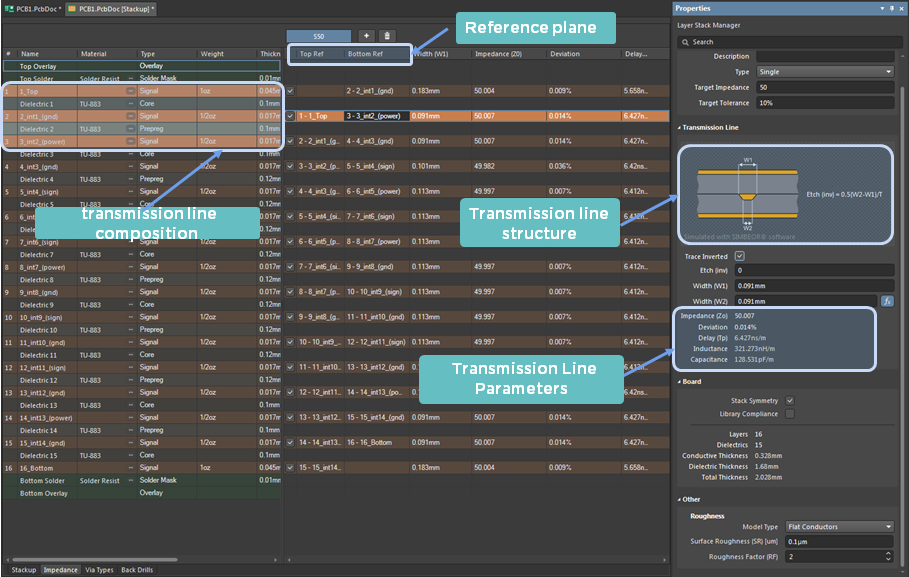
We've looked at the background and theory of transmission lines. Now we're going to look at how we actually conduct a transmission line impedance calculation in Altium Designer. The Layer Stack Manager (LSM) is your hub for impedance profiles definition. It is very important to have the Properties Panel open when using the LSM as it is used heavily in these operations. After you define your layer stack, you must define your Impedance Profiles in the tab of the LSM. You can think of an impedance profile as a definition for a particular type of transmission line. For example, when we saw the USB specification, we saw there were some defined 90 Ohm differential transmission lines. We can create 90 Ohm differential impedance profiles to ensure appropriate traces are created for your design.
In this instance, we have created a single ended signal with a default return path with the default name S50 (single ended signal 50 Ohm). Let’s take a deeper view of the impedance profile definition in a project. When you create your impedance profiles, you highlight the various layers to change layer parameters with the Properties Panel to refine the impedance to ensure alignment with your layer stack.
You can then apply these impedance profiles to your project and individual design rules. Before we do that, we want to talk about the types of transmission lines that we currently support in Altium Designer.
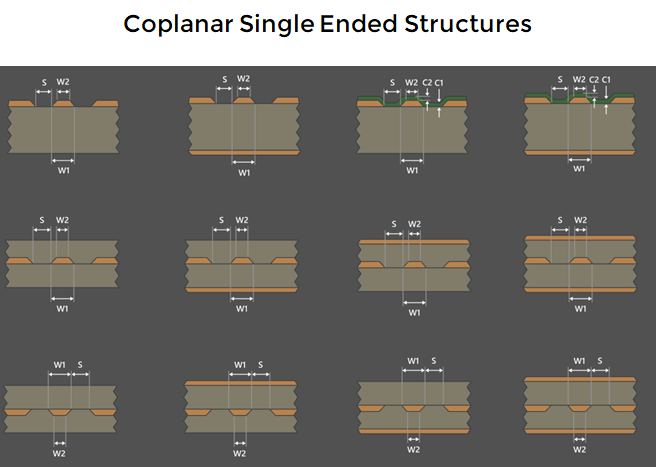
Transmission Line Types Available in Altium Designer
Single ended structures have a conductor with a return path. You can have the return path on another layer or on the same layer known as coplanar. Note that even the solder mask is taken into account because it has dielectric properties that can influence signal propagation. We also have coplanar single ended structures where the return path is on the same layer found on either side of the conductor.
Similarly, we have differential structure and coplanar differential signals.
Transmission Line Impedance Profile Setup
When you highlight your layer in your impedance profile, you immediately see your constituent layers in said profile. In this case, we have one dielectric 1 and 2 with internal ground and power on either side. Impedance on this layer will be automatically calculated with this profile and you will see the cross-section that the system will generate. When you set up an impedance, you're able to define the impedance value and the target tolerance gives you more wiggle room to have trace widths and topology that's going to work best for your design. We see the result in transmission line parameters in the Properties Panel. If we want, we can allow the system to just generate the trace it recommends for the given parameters or we can trace width we want for our layer. For example, define a 0.1 trace width and hit the fx button and it will calculate all parameters.
Assign Impedance Profile To Nets
Once you have your impedance profiles complete, you can go into your design rules to assign your impedance profiles to associated nets. This is where you'll ensure the impedance profile you created is used during routing to ensure your traces will have the correct impedance.
What's really nice about using these rules and impedance profiles is that if you decide you need to change the impedance profile, you change the profile once in the layer stack manager and it echoes to all of the associated rules that reference it. This is incredibly powerful over existing approaches where external calculators are used and individually annotated because you have the ability to update things quickly and uniformly. Best of all the retrace route functionality will update any existing routes to the proper trace thickness for your new impedance profile definition.
In the PCB Rules and Constraints Editor window, you can assign an impedance profile to specific nets by going to the Routing --> Width section and creating a new rule. Within this new rule, you can select a specific net, or use a query to specify multiple nets, and assign the impedance profile to that net.
You can also organize groups of nets into Net Classes (including into Differential Pair Classes), which will allow you to apply impedance profiles to groups of nets all at once. This helps you stay productive so that you don't need to go through a long list of traces and apply the same design rule to each.
If you're tired of other impedance calculators or you're still working out impedance formulas by hand, try using the transmission line impedance calculation features in Altium Designer®. You'll have a complete platform for design, layout, routing, and rules checking in a single program.
Now you can download a free trial of Altium Designer and learn more about the industry’s best layout, simulation, and production planning tools. Talk to an Altium expert today to learn more.
About Author
Related Resources
Related Technical Documentation
Table of Contents
- Introduction
- Impedance Profiles
- Current Electronics Development Trends
- Transmission Line Impedance Model
- Transmission Line Impedance Equation
- Types of Transmission Lines in a PCB
- How Conductor Geometry Influences Impedance
- Some Rough Approximations
- Transmission Line Impedance Calculation in Altium Designer
- Transmission Line Types Available in Altium Designer
- Transmission Line Impedance Profile Setup
- Assign Impedance Profile To Nets
Design to Release, Without the Friction
- Keep reviews tied to the right version
- Reduce handoff confusion and rework
- Spot sourcing and release risk earlier
- Work solo, share when needed
Get Started
Thank you, you are now subscribed to updates.