Using the New Select Filter When Selecting Objects in Altium Designer

Whether you are making changes or deletions one thing is for certain, you are going to be selecting a lot of design objects in your design as you work on it. Altium Designer has introduced the select filter that will make the task of selecting objects much easier than before. This enables you to configure your design session so that you can select specific object types to work on.
When you have an area in your schematic or PCB layout that is very congested, it can be difficult to select the specific objects that you want. In the past, you may have had to zoom in tight or tried other tricks. Now you can set your filter for the object type that you want to select and you will have much more precision in your selection efforts.
This article will be a good introduction to selecting design objects in general in Altium Designer. Not only will you learn about the select filter, but we’ll cover some of the basics of the different select functions as well. Equip yourself with an understanding of the tools you need to navigate the layouts and interfaces that you are working with.
Watch this related video about Cross Select Mode in Altium Designer and more guides on Altium Academy Youtube channel
The Basics: Selecting Objects in Altium Designer
To select design objects with Altium Designer, you can either click the left mouse button while hovering over the object or holding the left mouse button down and drag a selection rectangle over the object.
 The two versions of drag-select in Altium Designer; Select Within & Select Touching
The drag select function is quite similar in that you can either select only those objects that fall within the boundaries of the drawn rectangle or you can select anything that the drawn rectangle touches. You can see the difference in the two images above where the “Select Within” rectangle is drawn from left to right, and shows as a blue color, while the “Select Touching” rectangle is drawn from right to left showing as green.
This is a basic function in Altium Designer, but for those who have migrated from other CAD systems that didn’t have this feature, it is important to understand. New users may find themselves drawing rectangle after rectangle and yet are unable to select the similar objects that they are expecting to.
As an example, in the image below you can see that even though the select within a rectangle drawn from left to right does completely encapsulate the VCC symbol and its connecting wire, it only partially covers that transistor.
Here you see an example of the “Select Within” selection rectangle in Altium Designer
Because the select within the rectangle only partially covered the transistor, it did not get selected as you can see on the right side of the image above. The select within the rectangle is a great tool to use in situations where you need to specifically select certain objects. To select all design objects as in this example though, drag your rectangle from right to left to form the select touching rectangle instead.
Here you see an example of the “Select Touching” selection rectangle in Altium Designer
In the image above we used the select touching rectangle. As you can see the rectangle is touching the VCC symbol, the transistor, and the connecting wire. The select touching rectangle did its job though, and on the right side, you can see that all of the similar objects are selected and ready to be edited.
Often similar objects such as the transistor shown below have child objects associated with them. The transistor component is the parent object, while the displayed text is the child object. Using the select within rectangle we’ve encapsulated the text but not the component.
The transistor in this picture is only partially selected
As you can see the editing handles of the parent object, which is the transistor, are highlighted in white instead of color. This means that it has a child object selected even though the parent object itself is not. You can also see the green colored highlight around the text showing that these are the design objects that are selected. These selected text objects could be edited or moved, but the component cannot be edited because it is not the actual selected object.
On the left side of the image below, we used a select touching rectangle (drawing right to left) to select the parent component object. We drew a small rectangle so as to only touch the component in order to select it.
The transistor in this picture is fully selected
As you can see in the middle of the above image, we were successful in selecting the parent object which in this case is the transistor component itself. This allows us to move the component and its associated text (child) objects, or to delete the component completely as you can see on the right side of the image.
Using the Select Filter When Selecting Objects in Altium Designer
After you get a handle for selecting design objects, you can jump into using Altium Designer’s select filter. In the image below you can see the properties panel open in layout. You can click the “Panels” button in the lower right corner of the session window and then select “Properties” from the pop-up menu. Make sure you have nothing selected in the session window otherwise the properties menu will report on the properties of the selected object.
The Properties Menu in Altium Designer’s PCB layout session
As you can see in the image above, there are several object types that you can set the select filter for. “Components”, “Tracks”, and “Vias” are just a few of them. These are toggle buttons that you can click on and off. You also have the ability to toggle all the filter types at once by using the “All Objects” button.
The select filter will allow you to specify the object type that you want to select. This will help prevent selecting multiple objects in tight spaces. The select filter is also very similar to both the schematic editor and the layout editor. Commonality between the tools is one of the highlights of using Altium Designer.
The Select Filter menu in the schematic
In the image above, the select filter has been accessed in the schematic by clicking on the select filter icon in the Active Bar. This pops up a small menu that only contains the select filter buttons in it.
Another way to access the select filter is to dock the properties menu into a panel as shown in the image below. You can do this by pulling the properties menu over to the panel, in this case on the left side in the image below, and landing it there. Once docked, you can access the properties by clicking on its tab on the bottom of the panel. Not only will this give you quick access to the select filter, but of all the different settings in the properties menu as well.
The Properties menu with the select filters docked in a schematic panel
Select Menus and Helpful Keyboard Shortcuts
Using the select filter will be extremely helpful if you aren’t using it already, but you can use plenty of other ways to select similar objects in Altium Designer. The select menu can be accessed by either going to the Edit > Select pulldown menu or by using a shortcut key to bring up the select menu.
Many commands have shortcut keys assigned, and you can find out which key to use by looking at the pulldown menu. For example, in the Edit pulldown menu, the “S” is underlined for the “Select” menu signifying that it is the shortcut key. You can use the combination of “S” and the specific command shortcut key to immediately access the command that you want.
The Select menu in an Altium Designer layout session
In the image above we’ve used the “S” shortcut key to display the select menu in the layout editor. You can see the different select commands that are available to you. If you aren’t familiar with them, here are a few examples of some that can be very useful.
- Lasso Select: This command allows you to define the area to be selected by drawing it free-form. This is very useful for selecting objects that are oddly shaped or are in a non-rectangular pattern.
- Select All: Sometimes you just need to quickly select everything, and here’s the command for that. Once you memorize the shortcut (SA), it will become second nature.
- Select Net: This is a PCB layout only command (the schematic version is “Select Connection”) that will allow you to select all electrical objects associated with a net.
There are many more selection commands in both the schematic and layout sides of Altium Designer. Learning to use these commands along with the new select filter will give you a noticeable increase in your productivity as you use the tools. For example, the lasso select command, as shown below, can be extremely useful.
Here is an example of the lasso select command in the schematic editor
Get More Granular With Query Select
There is one other way to conditionally select objects in a schematic or in the PCB based on certain logical criteria, which the designer has freedom to specify. This is to use the query engine from inside the PCB editor. The query engine in Altium Designer allows a user to filter different objects in a selection based on several conditions:
- Filter by object type (track, via, pad, polygon, etc.)
- Filter by layer location
- Filter by presence in a room
- Filter by net class membership
- Filter by component class membership
After creating a query, you can apply Select/Deselect, Mask out, and Zoom viewing options to manage which objects remain selected by the query filter. The video below shows some examples where the query filter is used to select and modify some differential pairs with length tuning segments, but without requiring a complete re-route of the pairs. You can also read more about the Query Language in the Altium Designer Documentation.
Not a Coder? Use the Query Helper
Altium Designer also includes a Query Helper that can assist you in creating queries to use with the filtering tool. The Query Helper will walk you through the creation of the logical conditions needed to execute a query for filtering objects in the schematics or PCB layout (a similar function is used in the design rule editor). You can use the same query and filtering features when creating footprints. An example query created in the query helper is shown below. With this feature, you don't need to manually code out a query, you can generate it by clicking through the required logical conditions in a graphical window.
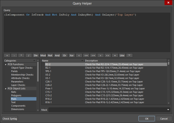
To access the Query Helper feature for filtering, select the option in the SCH Filter panel, PCB Filter panel (for PCB layouts), or in the SCHLIB Filter panel (for schematic symbols) or the PCBLIB Filter panel (for PCB footprints). Read more about accessing and using the Query Helper here.
When you want access to the industry's best CAD tools that help you speed up your design experience, use the PCB design tools in Altium Designer®. When you’re ready to release these files to your manufacturer, the Altium 365™ platform makes it easy to collaborate and share your projects.
We have only scratched the surface of what’s possible with Altium Designer on Altium 365. Start your free trial of Altium Designer + Altium 365 today.
Check out Altium Designer in action...
Powerful PCB Design

About Author
Related Resources


Related Technical Documentation


Table of Contents
Take advantage of the world's
most trusted PCB design system.
One interface. One data
model. Endless possibilities.
Effortlessly collaborate with
mechanical designers.
The world's most trusted
PCB design platform
Best in class interactive
routing
View License Options
Thank you, you are now subscribed to updates.