How to Panelize Your PCBs with Altium's PCB Panelizer

At a Glance
Whether you have PCBs to mass produce or boards to prototype, PCB panelization is efficient for production. Learn about Altium Designer's PCB panelizer.


Whether you have a slew of PCBs to mass produce for your customers or a handful of project boards you wish to prototype all in one simple swoop, PCB panelization is an effective way to bring high throughput and efficiency to PCB production.
In earlier days of PCB design, you would need additional software, hours of clunky engineering, and maybe even feasibility meetings with manufacturing teams for PCB panelization. However, today's PCB design software lets you easily prepare panels for a new design in much the same way as you would a single PCB. You can then prepare Gerber files for your PCB panel and other standard deliverables.
If you plan to create your own PCB panels and other output files before fabrication, take a look at our panelization tutorial in Altium Designer. We'll explore the advantages and disadvantages of panelizing on your own as a PCB designer, and how you can create your own PCB panels before fabrication.
- Should You Create Your Own PCB Panels?
- Best Practices for PCB Panelization
- Defining the Board Shape
- Placing PCBs in a Panel
- Placing Additional Boards

Should You Create Your Own PCB Panels with a PCB Panelizer?
The first point to note here is that not everyone will need to do PCB panelization. The manufacturer I most enjoy working with does not accept customer-created PCB panels; they do all panelization in-house. As a designer, I only need to worry about getting the design correct and ensuring that any output files from my design are error-free. If I've done that and my design passes a review, only then is it ready for panelization.
All the other points involved in transitioning a new design into fabrication can be performed by the fabricator. Their customers don't always get panels correct, even after being given a template or basic guidelines, and the fabricator ends up having to remake the PCB panels anyways. Therefore, fabricators may just bring that service in-house and build the cost into their NRE charge (regardless of whether you're using a turnkey solution).
The result is reduced liability for the designer; the fabricator takes full responsibility if the PCB panel is incorrect. The other advantage is reduced time for the designer; you just don't need to worry about building panels unless the board is larger than standard panel sizes. It also affects my pricing if I need to manage manufacturing for a client; I don't have to bring up my price for hourly NRE charges just to create PCB panels or other fab drawings that the fabricator might not need. Instead, I just pass on a flat fee to the customer and everyone is happy.
Best Practices for PCB Panelization
If you do plan to create your own panels and send them into fabrication, or you're a manufacturer and you'll need to do this in a new PCB design software package, then there are some basic points to note for panel design.
- The simplest guideline that is often overlooked is setting the standard panel size. Be sure to check with your fabricator on their panel sizes.
- Remember, finished circuit boards are being cut out of the panel, so your panel needs to have the exact same stackup as your boards.
- Take note of how the boards will be removed from a panel (tab routing, V-groove). You'll need to design these features into the panel. Read this project article to see how you can add route profiles to your PCB before panelization.
- Watch for clearances to the board edge; the board edge clearances you used in your PCB layout might be too shallow to allow for handling. A typical rule is to allow 0.5 in. edge clearance for double-sided boards and a 1 in. for multilayer boards.
- Don't forget about internal board spacing, which could be as small as 0.1 in., depending on breakout method.
- If the boards are going through pick-and-place and wave solder assembly, you need to add sufficient support to prevent accidental breakout.
With that out of the way, keep reading for a PCB panelization tutorial in Altium Designer.
Defining the Board Shape for PCB Panels
As mentioned above, the PCB panel needs to have the correct size before we start placing PCBs in the panel. To get started, you need to create a blank PCB document; this can be added to whichever project you’re working on, or it can be placed in its own project. To do this, simply right click on your project, navigate to ‘Add New to Project’ then select ‘PCB.’
Once you've created the blank PCB for your panel, you need to define the layer stack for the panel. Open up the Layer Stack Manager and define your layer thicknesses, plane layers, dielectric constant, etc. An easy way to do this is to export the layer stack details from your finished PCB layout as a .STACKUP file and import it as a template into the PCB for your panel.
After defining the layer stack, we can define the PCB panel size. As we showed in an earlier article, we can easily define any board shape we want by simply tracing out a shape over the top of our placements. Finally, you’ll benefit from setting an origin by navigating to ‘Edit’ > ‘Origin’ > ‘Set.’ Here is what we should see:
Blank PCB document.
Placing PCBs in a Panel
For this example, I'll use a previous PCB file from a past tutorial. To place a board in the sized panel, navigate to ‘Place’ > ‘Embedded Board Array/Panelize’ which will present you with a blank rectangle and some crosshairs. This is simply a placeholder, and we need to specify the board we want to place.
By pressing ‘Tab’ during the placement period, the program will pause to give us a prompt to specify some parameters for our placement. You can also escape out of the placement tool and double-click on the placeholder. This will open up a dialog that allows you to select the PCB you want to place as an array. You can then enter dimensions for each board in the array, as well as the number of rows/columns for repeating the PCB placement in the panel.
Embedded board array window.
Notice that each board here is linked rather than simply copy/pasted. This is huge when it comes to deep design edits in that it makes integrating each file together a breeze. Rather than having to edit each child document, Altium Designer takes care of this for you.
Here is what I have now:
Vertically placed PCBs.
Placing Additional Boards
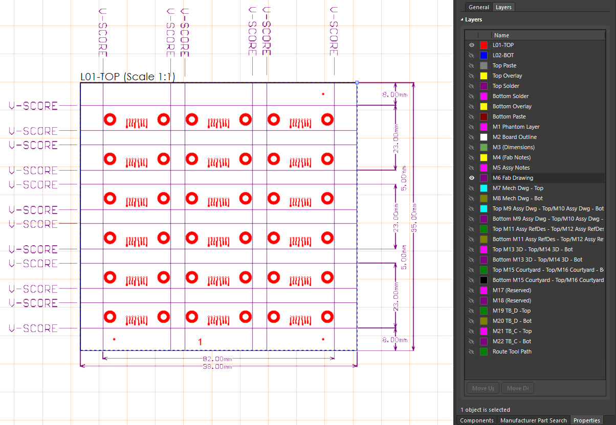
Instead of placing a vertical stack of boards here, let’s assume I want to place another board vertically next to my existing three boards. Maybe this is another design that you just want to toss into the manufacturing batch, maybe you are working with limited printing space, whatever the reason, you can pick and place as many various boards as you wish.
With the same process as used above, we’ll use a slightly different placement location and design. We can place additional boards rotated 90 degrees if we like. Here is what I’ve decided to do (we’ll assume I’m working with a smaller space, but still need to fit four boards onto one print):
Vertically placed PCBs with one skewed.
At this point, you can move groups of PCB panels around the board and set the required edge clearances. For a more advanced tutorial on creating dimensioned panel drawings with multiple boards, take a look at this recent blog article. Once the panel is defined and board layouts are placed, you’ve gone as far as you need for your PCB panelization.
DFM For PCB Panels
The preceding example shows how boards can be added to a panel using the embedded board array, but it is still a bit contrived. In reality, panels require a bit more detail in order to be useful for manufacturing. When creating a panel, the designer or manufacturer needs to incorporate tooling into the panel design. This will enable the manufacturer to properly handle the panels and deeply analyze each PCB. Typically, panels will include at least the following elements:
- Tooling and mounting holes for fixation
- Detachable rails around the edge of the panel
- Lines drawn for the grooves or routing/milling paths
- Mouse bites for manual removal from the panel
- Additional detail in a silkscreen layer, such as panel part number
- Panel fiducials to determine the mobile orientation of the panel
- Layer numbers in copper on the tooling rails
- Stacking stripes at the tooling rail edge
A PCB manufacturer will build their panel from your artwork using CAM software. However, there is nothing prohibiting a designer from creating a custom panel, and this can be done in Altium Designer.
If you're designing your own panel, contact your PCB fabrication house for their panel requirements or a template. They will specify several elements, such as tooling rail size along the outside of the panel. One of the more important elements that is defined by the fabricator is routing tool sizes for paneling the PCBs. Alternatively, if scoring will be used to remove the PCBs, the fabrication house will specify a clearance around the scoring path. They may also have constraints on sizing and placement of mouse bites on each PCB in the panel.
PCB Panel Drawings
When a panel is designed, it will also need a corresponding fabrication drawing. Almost all of the information in a PCB panel drawing is the same as that required in a fabrication drawing for an individual PCB. You will need to include a set of notes for the panel drawing which will function as the master fabrication data for your panel.
A PCB panel drawing can be created in Altium Draftsman, similar to the process for a single PCB. Normally, to create a panel layout, you add a new PcbDoc file to your project. To link your Draftsman document to your panel drive, select the PcbDoc file for your panel in the properties panel inside the Draftsman document.

The PcbDoc with the panel can then be placed in the Draftsman document as a drill drawing view, assembly view, Gerber layer view, or any of the other views that are auto-generated inside of Draftsman. Because the panel drawing is essentially a PCB fabrication document, it should also include the other fabrication elements you would expect in such a drawing:
- Complete fabrication notes
- A drill table for each layer span or lamination
- Specification for depanelization
- Stackup drawing or description
- Callouts for milled slots with tolerances
Export as a DXF/DWG File
I've shown in one video that Altium Draftsman is not your only option to create fabrication drawings. You can still create a fabrication drawing with an embedded board array in a PcbDoc file as a mechanical layer. Just like you would do in AutoCAD, you can draw out the Title Block and border for a fabrication/assembly drawing as a mechanical drawing using the standard drawing tools in Altium Designer inside the PcbDoc file. Whenever I need to do this, I always do it in the Drill Drawing layer. This way, you only have a single layer you will need to export as your DXF/DWG file, rather than combining separate mechanical layers and configuring them in AutoCAD or another drafting application.

This embedded board array is placed in a PcbDoc file with a title block, drill table, and fabrication notes included in the drill layer. An OutJob file can then be used to export the fabrication drawing as a PDF file, or the File --> Export --> DWG/DXF command can be used to create a DWG/DXF file.
This is a great option for companies that need to share the fabrication drawing with other engineers or designers who are not PCB design software users. For example, MCAD users can take a fabrication drawing and match it up with their mechanical designs when they have a DXF file. In another example, manufacturing engineers or process engineers can use the DXF export directly to plan fabrication or assembly steps for the PCB, enclosure, and any other mechanical elements. This capability gives the design team flexibility to create a drawing in a vendor-neutral format that can be viewed by anyone on a design team.
With the CAD and CAM features in Altium Designer, you can fully define your panelized board and prepare all your other deliverables for your manufacturer. Additionally, with the integration between design files and panelized files, it's easy to make board edits and panel updates without remaking your panel. Once you're ready to deliver your design files, you use the Altium 365 platform to share your project with your manufacturer and collaborators.
Would you like to find out more about how Altium can help you with your next PCB design? Talk to an expert at Altium.

About Author
Related Resources


Related Technical Documentation

Thank you, you are now subscribed to updates.


