


Erschließen Sie das komplette Systemdesign mit Altium Designer 24
In einer sich schnell entwickelnden technologischen Landschaft ist die Fähigkeit, hocheffiziente und anpassungsfähige elektronische Systeme zu entwickeln, von größter Bedeutung. Wenn Sie die Leistungsfähigkeit von Funktionalitäten wie Kabelbaum-Design, Multi-Board-Design und MCAD CoDesigner nicht nutzen, riskieren Sie erhebliche Rückschläge bei Ihren Projekten. Der Verzicht auf diese Tools kann zu verpassten Terminen, einer erhöhten Anzahl von Design-Fehlern und einer mangelnden Synchronisation zwischen elektrischen und mechanischen Aspekten führen und letztendlich den Gesamterfolg des Projekts beeinträchtigen.
Sind Sie bereit, jede Design-Komplexität zu bewältigen? Altium Designer 24 bietet Ihnen die Möglichkeit, Ihren Ansatz zu revolutionieren. Melden Sie sich jetzt an, um zu sehen, wie Altium Designer 24 mit MCAD CoDesigner umfassende Lösungen für das Design von Kabelbäumen, Multi-Boards und die Kollaboration mit Mechanik-Designern bietet.
NEHMEN SIE AN UNSEREM WEBINAR TEIL, UM FOLGENDES ZU LERNEN:
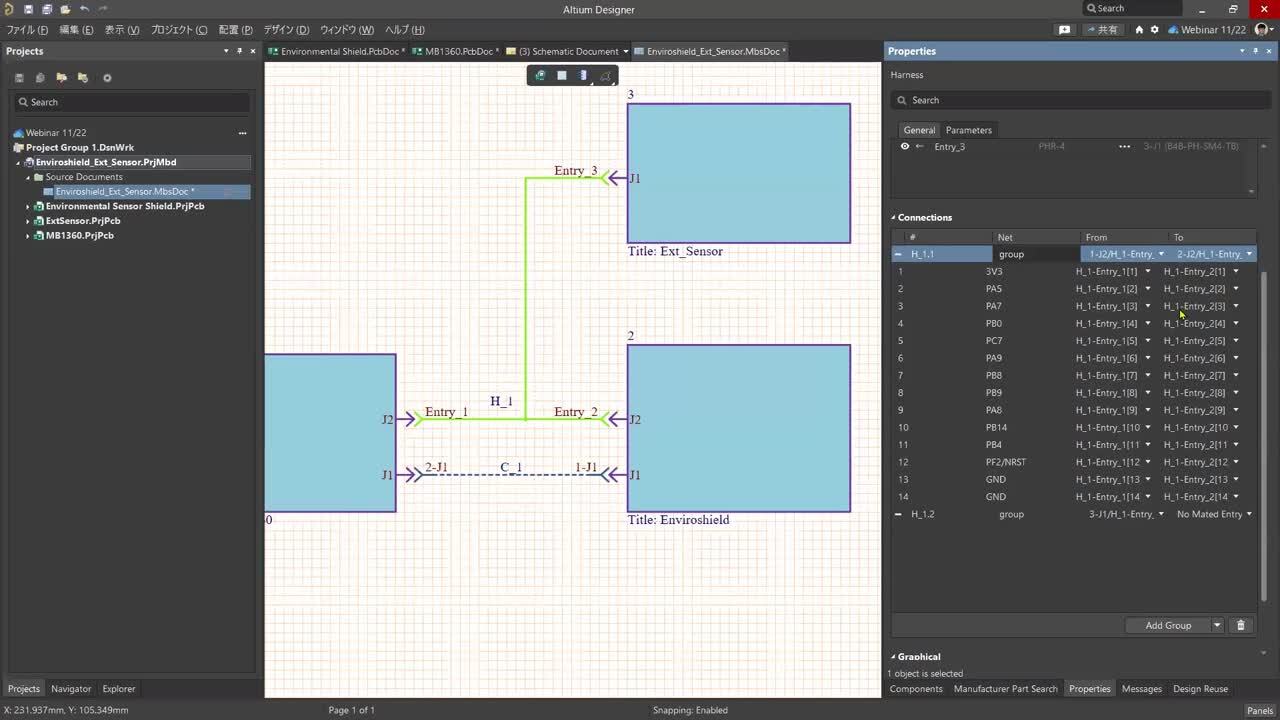
- Kabelbaum-Design in Altium Designer 24
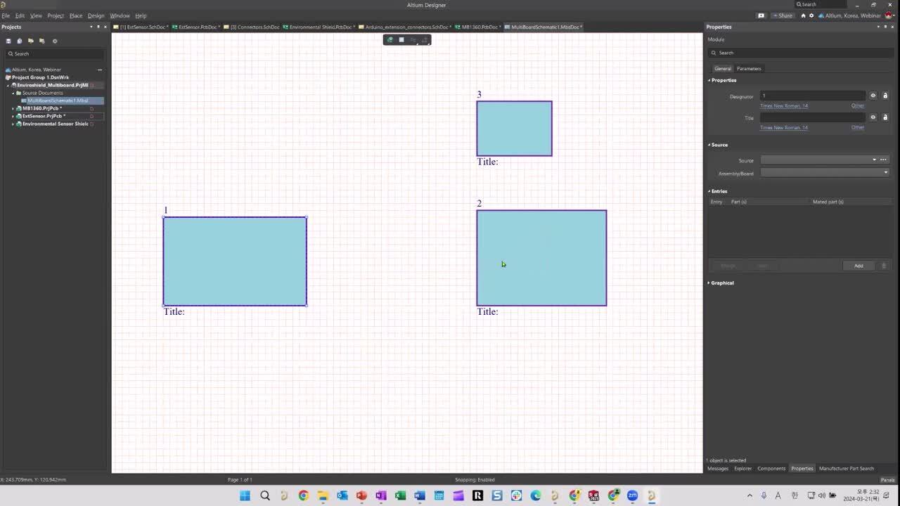
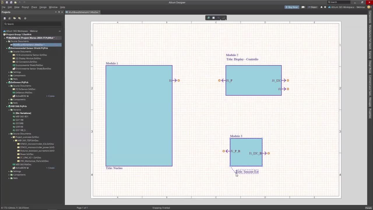
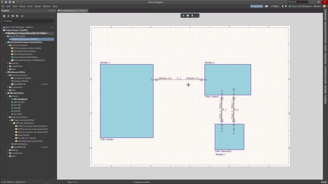
- Multi-Board-Design in einer einheitlichen Umgebung
- Nahtlose Integration mit MCAD CoDesigner

Registration has recently closed. Check back soon for on-demand webinar.
Related Technical Documentation
Ähnliche Resourcen
Erschließen Sie das komplette Systemdesign mit Altium Designer 24
Erstellt: March 27, 2024

At a Glance
Nehmen Sie an diesem Webinar teil, in dem Sie wertvolle Einblicke in die Optimierung Ihres Design-Workflows, die Steigerung der Produktivität und die Überwindung der häufigsten Herausforderungen bei Multi-Board-Design-Projekten erhalten.


-
 Präsentiert von Martin Malenica - Field Application Engineer
 00:22:58
•
Mar 28, 2024
Präsentiert von Martin Malenica - Field Application Engineer
00:22:58
•
Mar 28, 2024
00:22:58
•
Mar 28, 2024
Präsentiert von Martin Malenica - Field Application Engineer
00:22:58
•
Mar 28, 2024
-
 Hosted by Alex Hall - Technical Marketing Engineer
00:33:46
•
Mar 22, 2024
Hosted by Alex Hall - Technical Marketing Engineer
00:33:46
•
Mar 22, 2024
Hosted by Alex Hall - Technical Marketing Engineer
00:33:46
•
Mar 22, 2024
Hosted by Alex Hall - Technical Marketing Engineer
00:33:46
•
Mar 22, 2024
-
 Hosted by Aida Gharahkhani - Field Application Engineer
00:48:52
•
Mar 21, 2024
Hosted by Aida Gharahkhani - Field Application Engineer
00:48:52
•
Mar 21, 2024
Hosted by Aida Gharahkhani - Field Application Engineer
00:48:52
•
Mar 21, 2024
Hosted by Aida Gharahkhani - Field Application Engineer
00:48:52
•
Mar 21, 2024
-
 Présenté par Nourhene Kerkeni - Field Application Engineer
00:33:36
•
Mar 29, 2024
Présenté par Nourhene Kerkeni - Field Application Engineer
00:33:36
•
Mar 29, 2024
Présenté par Nourhene Kerkeni - Field Application Engineer
00:33:36
•
Mar 29, 2024
Présenté par Nourhene Kerkeni - Field Application Engineer
00:33:36
•
Mar 29, 2024
-
 오힘찬 FAE 발표
00:40:11
•
Mar 25, 2024
오힘찬 FAE 발표
00:40:11
•
Mar 25, 2024
오힘찬 FAE 발표
00:40:11
•
Mar 25, 2024
오힘찬 FAE 발표
00:40:11
•
Mar 25, 2024
-
 Presentato da Manuel Valero - Field Application Engineer
00:47:54
•
Mar 25, 2024
Presentato da Manuel Valero - Field Application Engineer
00:47:54
•
Mar 25, 2024
Presentato da Manuel Valero - Field Application Engineer
00:47:54
•
Mar 25, 2024
Presentato da Manuel Valero - Field Application Engineer
00:47:54
•
Mar 25, 2024
-
 Presentado por Manuel Valero - Field Application Engineer
00:47:27
•
Mar 22, 2024
Presentado por Manuel Valero - Field Application Engineer
00:47:27
•
Mar 22, 2024
Presentado por Manuel Valero - Field Application Engineer
00:47:27
•
Mar 22, 2024
Presentado por Manuel Valero - Field Application Engineer
00:47:27
•
Mar 22, 2024
-
 プレゼンター:ダニエル チョウ
01:07:41
•
Mar 20, 2024
プレゼンター:ダニエル チョウ
01:07:41
•
Mar 20, 2024
プレゼンター:ダニエル チョウ
01:07:41
•
Mar 20, 2024
プレゼンター:ダニエル チョウ
01:07:41
•
Mar 20, 2024
Product:
Multiboard-PCB-Design
Harness Design
Altium Designer
Webinare
Elektroingenieure
Systems and Product Design
Other Recordings
In einer sich schnell entwickelnden technologischen Landschaft ist die Fähigkeit, hocheffiziente und anpassungsfähige elektronische Systeme zu entwickeln, von größter Bedeutung. Wenn Sie die Leistungsfähigkeit von Funktionalitäten wie Kabelbaum-Design, Multi-Board-Design und MCAD CoDesigner nicht nutzen, riskieren Sie erhebliche Rückschläge bei Ihren Projekten. Der Verzicht auf diese Tools kann zu verpassten Terminen, einer erhöhten Anzahl von Design-Fehlern und einer mangelnden Synchronisation zwischen elektrischen und mechanischen Aspekten führen und letztendlich den Gesamterfolg des Projekts beeinträchtigen.
Sind Sie bereit, jede Design-Komplexität zu bewältigen?

Author
Author
Martin Malenica has a masters in electronic and computer engineering at the University of Zagreb. His previous experience consists of multiple embedded systems positions at robotics start-ups (Gideon with USD 35m in Seed and Series-A funding) and SMEs. His engineering strengths lie in system architecture, PCB design and embedded programming. Aside from engineering, Martin has spent the last 1.5 years working at a leading European management consulting firm, where he focused on strategies to support large OEMs and Tier-1s regarding the current semiconductor shortage across the whole EMEA region. Martin has practical experience within AD, but also a good understanding of competitor tools, especially on the procurement and supply chain side, like Everstream, Resilinc, Silicon Expert, Z2Data etc. Martin Joined Altium in 2023 as part of the Technical Sales team in Germany.

Author
Author
Alex has a background in electrical engineering and a strong passion for technical marketing. Graduating with a bachelor’s in electrical engineering from Clemson University in 2018, he has since excelled in various roles within the technology sector. Starting his career at Kyocera AVX, Alex served as an RF Field Applications Engineer, establishing strong client relationships and designing passive bandpass filters and antenna systems. He then transitioned to TDK as an Account Executive, where he provided sales and technical support, leading a dynamic sales team and offering design assistance to customers. Currently, Alex is a Technical Marketing Engineer at Altium, leveraging his technical expertise to develop marketing materials.

Author
Author
Aida works as a Technical Sales Engineer at Altium and is based in the Sydney, Australia office. Aida studied Electrical/Electronic Engineering and completed Master of Engineering (MEng) Field of Mechatronics, Robotics, and Automation Engineering from the University of Western Sydney (UWS). Aida also completed certificates in Microcontroller Programming, Project Management Principles and Practices Specialization from the university of UC Irvine California. Aida has experience as an Electrical Engineer, Business Development Manager, Project Manager, Operations Manager, most recently in the last 10 years prior to joining Altium working in Engineering Process improvement. The most important thing that she always focuses on in her career is communication and trust. Aida strongly believes that communication is the solvent of all problems, when the trust accountability is high, communication is easy, instant, and effective.

Author
Author
Nourhene is an Electronic Engineer specializing in PCB Design and FPGA Programming, holding a Master’s degree in RFID technologies. Since joining Altium in 2019, she has partnered closely with the sales team to support both prospects and existing customers through technical sales and marketing initiatives across Altium’s portfolio.
Before Altium, Nourhene designed complex PCBs for Automotive and Aerospace applications at large international companies, where she also managed comprehensive testing processes. She has extensive experience collaborating with PCB manufacturers across Europe and Asia. Nourhene holds CID certification and is a certified Altium Designer Trainer.

Author
Author
Aiden은 대학에서 전자공학을 전공하였으며 PCB 설계 분야의 R&D로 7년 이상의 경험을 가지고 있습니다. 그는 전자 제품을 위한 SMPS, 인버터, 컨버터 설계 경험이 있습니다. 제품 프로젝트를 이끌었으며 설계, 관리, 인증 제품 테스트와 같은 모든 작업을 경험했습니다. 그리고 한국 리셀러(Hancom Intelligence) 팀에서 4년 이상 Altium Designer 사용자들을 위한 기술 지원 및 교육을 제공했습니다. Concord Pro와 Altium 365를 사용하여 PLM 요구 사항에 대한 컨설팅 및 지원을 했습니다. 또한 Altium Designer에 대한 수십 차례의 교육 및 웨비나를 경험했습니다.
Aiden은 2022년 11월부터 Altium에서 기술 영업 엔지니어로 근무하고 있으며 현재 한국 사무소에 근무하고 있습니다.

Author
Author
Manuel Valero is an Electronics Engineer with experience ranging from his own repair and IT businesses to working with multinational companies in the semiconductor and passive components branches; he has covered diverse roles like Repair Engineer, Product Engineer, Testing Engineer, Design Engineer, Product Marketing Engineer, FDE, etc.
He has quite varied interests, not just the electronics area; this go from bicycle riding, swimming, wandering, astrophysics, physics, biology and a long etcetera.
Having worked and lived in several countries, he finds himself comfortable in multicultural environments and enjoys working with customers.

Author
Author
Daniel joined Altium in 2019 as an Application engineer and moved into the Technical Sales role in the same year. Daniel provides technical assistance for sales, third party distributors, and customers in the Asia Pacific region (APAC) and is based in the Altium Tokyo, Japan office. Daniel has experience with PCB, FPGA, and ASIC design in telecommunication and Information industries.
Related Technical Documentation
Ähnliche Resourcen
Vom Entwurf bis zur Freigabe – ganz ohne Reibungsverluste
- Prüfungen an die richtige Version binden
- Verwirrung bei Übergaben und Nacharbeit reduzieren
- Beschaffungs- und Freigaberisiken früher erkennen
- Allein arbeiten, bei Bedarf teilen
Erste Schritte
Platform-based Solutions
Tools
Lösungen
Unternehmen
Karrieremöglichkeiten
© 2026
Altium Pty. Ltd.