Skip to main content
Mobile menu
Solutions
Octopart Discover
Go beyond part search to discover viable solutions, evaluate tradeoffs, and make better decisions earlier
Altium Develop
Design advanced PCBs in Altium Designer, working independently or connecting reviewers, sourcing data, and release coordination when needed
Altium Agile Teams
Bring structure to multidisciplinary electronics development and collaboration without sacrificing speed
Altium Agile Enterprise
Connect context from intent through release with an intelligent, governed, extensible platform
Resources & Support
Free Altium 365 Tools
Gerber Compare
Online PCB Viewer
Resources & Support
Learning Hub
Support Center
Documentation
Webinars
Altium Community
Forum
Bug Crunch
Ideas
Education & Training
Student Lab
Free access to professional PCB design software, training, and learning resources for students
Educator Center
A comprehensive education platform providing curriculum, software, training, and classroom resources for educators
Altium Education Curriculum
Free college- and university-level PCB design curriculum designed to prepare students for real-world engineering careers
Altium Professional Training
Flexible on-demand and instructor-led training courses that help engineers build and advance their PCB design skills
Search Open
Search
Search Close
Sign In
Main menu
Home
PCB Design
Collaboration
Component Creation
Data Management
Design Outputs
ECAD/MCAD
HDI Design
High Speed Design
Multi-Board
PCB Layout
PCB Routing
PCB Supply Chain
Power Integrity
RF Design
Rigid Flex
Schematic Capture
Signal Integrity
Simulation
Software
Develop
Discover
Agile
Altium 365
Altium Designer
Education
Programs
Altium Academy
Engineering News
Guide Books
Newsletters
Podcasts
Projects
Training Courses
Webinars
Whitepapers
Home
Altium Experts
About Author
Recent Articles
Impedance Calculations for Transmission Lines
1 min
Webinars
Today’s PCBs contain many transmission lines. Combine this with increased clock frequencies and data rates and the result is a
Read Article
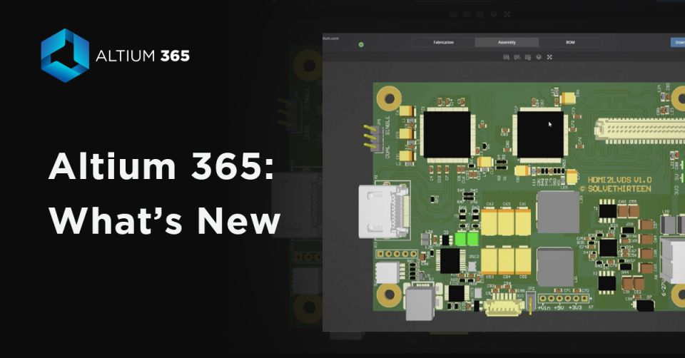
What's New: Altium 365 November 2021 Updates
3 min
What's New
Check out the latest developments and new features on Altium 365. Open Beta features include Schematic Compare, Gerber Compare, MCAD CoDesigner Updates, and more. Read now to learn more.
Read Article
Increase Productivity With Easy Component Creation
1 min
Webinars
Component creation is a necessary evil when it comes to design, and it’s something we all need to do. But
Read Article
Increase Productivity With Easy Component Creation
1 min
Webinars
Component creation is a necessary evil when it comes to design, and it’s something we all need to do. But
Read Article
Increase Productivity With Easy Component Creation
1 min
Webinars
Component creation is a necessary evil when it comes to design, and it’s something we all need to do. But
Read Article
Increase Productivity With Easy Component Creation
1 min
Webinars
Component creation is a necessary evil when it comes to design, and it’s something we all need to do. But
Read Article
Pagination
First page
« First
Previous page
‹ Previous
Page
34
Current page
35
Page
36
Page
37
Page
38
Page
39
Next page
Next ›
Last page
Last »