Skip to main content
Mobile menu
Discover
Develop
Agile
Resources & Support
Free Altium 365 Tools
Gerber Compare
Online PCB Viewer
Resources & Support
Learning Hub
Support Center
Documentation
Webinars
Altium Community
Forum
Bug Crunch
Ideas
Education
Student Lab
Educator Center
Altium Education Curriculum
Search Open
Search
Search Close
Sign In
Main menu
Home
PCB Design
Collaboration
Component Creation
Data Management
Design Outputs
ECAD/MCAD
HDI Design
High Speed Design
Multi-Board
PCB Layout
PCB Routing
PCB Supply Chain
Power Integrity
RF Design
Rigid Flex
Schematic Capture
Signal Integrity
Simulation
Software
Develop
Discover
Agile
Altium 365
Altium Designer
Education
Programs
Altium Academy
Engineering News
Guide Books
Newsletters
Podcasts
Projects
Training Courses
Webinars
Whitepapers
Meeting Standards: IPC 6012 Class 3 Via Sizes and Annular Rings
Take a look at the above image of a PCB layout, specifically the vias and drill holes poking through the silkscreen. It's quite clear that some of these vias are off-center, meaning the drill hit that created these vias was not dead-center in the receiving land. This leaves behind an annular ring, something which might be considered a defect in certain IPC product classes. Under the IPC standards for rigid boards, we have several possible
Read Article
When to Use Tented vs. Untented Vias in Your PCB Layout
Some designers swear by tented vias and prefer to always use them. When should these be used and when should they be avoided? We’ll explore in this article.
Read Article
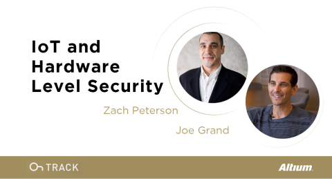
Design Your Electronic Device with Hacking in Mind
A very eye-opening world of hacking and understanding the never-ending risk to secure your electronic device. You wouldn’t want to miss this episode with a famous “good hacker” Joe grand. Watch now or listen on the go.
Read Article
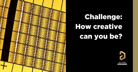
SAP (Semi-Additive PCB Process) – How Creative Can You Be?
Challenge how creative you can be! Can SAP processes produce plated through vias? Read this article to find out!
Read Article
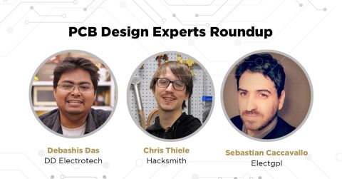
PCB Design - Fun, Frustration and Misconception
What do the top minds in the PCB Design social media space think about the modern landscape? We sat down with Hacksmith Industries, DD ElectroTech, and Electgpl to chat about how they got started, what frustrates them, what they think about A.I., and much more. Chris Thiele - Hacksmith Entertainment Ltd. So I think the most challenging design I've ever made was a Daft Punk helmet, Guy-Manuel. I designed several boards for that project, and they
Read Article
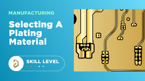
How to Choose Board Plating and Thickness for Your PCB
Ever wondered what surface plating you should use? We've compiled important data on PCB plating.
Read Article
What's HDI? Design Basics and the HDI PCB Manufacturing Process
Learn about design basics for HDI PCB design. When planning for the HDI PCB manufacturing process, you can prepare accurate designs and deliverables with Altium.
Read Article
Recover Conductor Losses By Clearing Your PCB Ground Layer
Need to recover some conductor losses? Here’s how clearing out your ground plane near an I/O or connector can help.
Read Article
Pathological Design Features: Eric Bogatin on PCB Design
Our podcast all-time favorite podcast guest is back to help PCB designers recognize bad PCB design guidelines. Tune in and listen on the go now.
Read Article
All About PCB-Mount Transformers
Before you rectify your AC input down to DC, you’ll need to step down your mains power to the desired voltage with a PCB-mount transformer.
Read Article
Pagination
First page
« First
Previous page
‹ Previous
…
Page
120
Page
121
Page
122
Page
123
Current page
124
Page
125
Page
126
Page
127
Page
128
…
Page
130
Page
140
Page
150
Page
160
Page
170
Page
180
Page
190
Page
200
Page
210
Page
220
Page
320
Page
420
Next page
Next ›
Last page
Last »
Subscribe to