Skip to main content
Mobile menu
Discover
Develop
Agile
Resources & Support
Free Altium 365 Tools
Gerber Compare
Online PCB Viewer
Resources & Support
Learning Hub
Support Center
Documentation
Webinars
Altium Community
Forum
Bug Crunch
Ideas
Education
Student Lab
Educator Center
Altium Education Curriculum
Search Open
Search
Search Close
Sign In
Main menu
Home
PCB Design
Collaboration
Component Creation
Data Management
Design Outputs
ECAD/MCAD
HDI Design
High Speed Design
Multi-Board
PCB Layout
PCB Routing
PCB Supply Chain
Power Integrity
RF Design
Rigid Flex
Schematic Capture
Signal Integrity
Simulation
Software
Develop
Discover
Agile
Altium 365
Altium Designer
Education
Programs
Altium Academy
Engineering News
Guide Books
Newsletters
Podcasts
Projects
Training Courses
Webinars
Whitepapers
PCB Design Review Checklist
It’s essential to check a board for issues before production or prototyping. Here’s an extensive checklist you can adapt or use directly for PCB design review.
Read Article
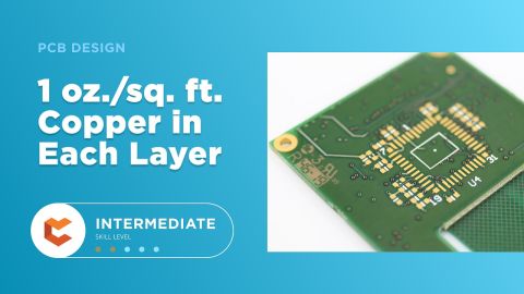
Do You Always Need 1 oz. Copper Thickness on Each Layer?
1 oz. copper thickness is often seen as a standard thickness value used in many designs. Here’s when you might need thicker copper on every layer.
Read Article
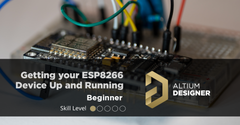
Getting Started With ESP8266
A project overview on getting started with the ESP8266 device. Expert Ari Mahpour reviews the benefits of using a device such as the NodeMCU board from HiLetgo and how to get up and running with a few examples.
Read Article
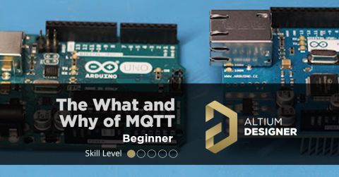
Getting Started with MQTT and Arduino Uno
Check this out. This is a new project overview demonstrating MQTT by expert Ari Mahpour. In this article, Ari answers the What and Why of MQTT, and gives guidelines to get your project started.
Read Article
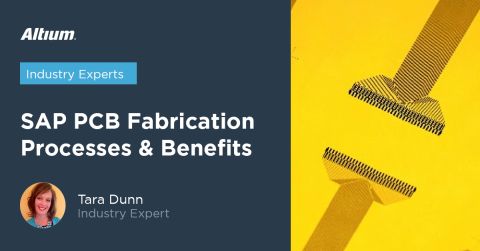
SAP (Semi-additive PCB process): The Basics
Expert Tara Dunn answers what are semi-additive PCB fabrication processes and what are the benefits? Read now and learn more about SAP.
Read Article
Can You Route Digital Signals on a 2-layer PCB Design?
2-layer PCBs are a common entry-level choice for designers, and they can even support high speed designs if built correctly.
Read Article
Deterministic Solutions to Solve Skew Problems
Avoid getting your design "skewed"! Today's guest is Z-Zero's Founder and CEO, Bill Hargin. Together we will dive into the cause of getting skews in your board. Watch now to get answers to your "skews" questions.
Read Article
Two 4 Layer PCB Stackups With 50 Ohms Impedance
Need a 4-layer PCB stackup that can support high speed components on both sides of the board? Consider these alternatives to the typical 4-layer stackup.
Read Article
Design to Manufacturing with a Single Mouse Click
Imagine if you could design your circuit board, run simulations, source your parts, generate an accurate BOM, generate your output files and simply press a “send to manufacturing” button all within your design environment? While that may sound like a far-off dream, this interview with Misha Govshteyn from MacroFab will give you insight into how they are partnering with Altium to make this dream a reality very soon. Judy Warner: Misha, please
Read Article
Microstrip PCB Ground Clearance Part 2: How Clearance Affects Losses
In a previous article, I provided a discussion and some simulation results on the necessary clearance between impedance controlled traces and nearby grounded copper pour. What we found was that, once the spacing between the pour and the trace becomes too small, the trace becomes an impedance-controlled coplanar waveguide (with or without ground). We also saw that the 3W rule for the spacing between the trace and the grounded copper pour is a bit
Read Article
Pagination
First page
« First
Previous page
‹ Previous
…
Page
124
Page
125
Page
126
Page
127
Current page
128
Page
129
Page
130
Page
131
Page
132
…
Page
140
Page
150
Page
160
Page
170
Page
180
Page
190
Page
200
Page
210
Page
220
Page
230
Page
330
Next page
Next ›
Last page
Last »
Subscribe to