Skip to main content
Mobile menu
Discover
Develop
Agile
Resources & Support
Free Altium 365 Tools
Gerber Compare
Online PCB Viewer
Resources & Support
Learning Hub
Support Center
Documentation
Webinars
Altium Community
Forum
Bug Crunch
Ideas
Education
Student Lab
Educator Center
Altium Education Curriculum
Search Open
Search
Search Close
Sign In
Main menu
Home
PCB Design
Collaboration
Component Creation
Data Management
Design Outputs
ECAD/MCAD
HDI Design
High Speed Design
Multi-Board
PCB Layout
PCB Routing
PCB Supply Chain
Power Integrity
RF Design
Rigid Flex
Schematic Capture
Signal Integrity
Simulation
Software
Develop
Discover
Agile
Altium 365
Altium Designer
Education
Programs
Altium Academy
Engineering News
Guide Books
Newsletters
Podcasts
Projects
Training Courses
Webinars
Whitepapers
Silicon Photonics Integration Challenges in PCB Design
Silicon photonics will use the same manufacturing processes used in silicon ICs I was honored to meet Richard Soref at a recent IEEE conference and discuss the current state of electronic-photonic integrated circuits (EPICs). The man is often called “the Father of Silicon Photonics”, and for good reason. If you ask him nicely, he’ll tell you how to build all the fundamental logic gates as photonic circuits directly on silicon. Now is a landmark
Read Article
Flex Circuit Specific Terms and Definitions
Learn key flex circuit terms and definitions to navigate flex and rigid-flex PCB design with confidence. Master industry terminology for better designs.
Read Article
Stacking The Odds In Your Favor: Mastering The Art of Stackup Design
As everyone knows, the PCB stackup is the substrate upon which all design elements are assembled. And, it is incumbent upon the product development engineer to own the PCB stackup process which includes calling out the exact type of laminate, prepreg and copper needed in every layer of the stackup as well as taking into account all of the electrical characteristics of the PCB to ensure a design that is fully functional from both a mechanical and
Read Article
It’s Your Loss: Determining And Controlling Loss In The PCB Design Process
When it comes to designing a high-speed PCB, we always have to factor in the dynamic of signal loss. And, there are lots of areas where loss can occur. Accounting for all of these aspects of loss can be a challenging and time-consuming task as too much loss can prevent a high-speed PCB from functioning properly. This article will address the various aspects of loss, how they factor into the PCB design process, and how loss can be effectively
Read Article
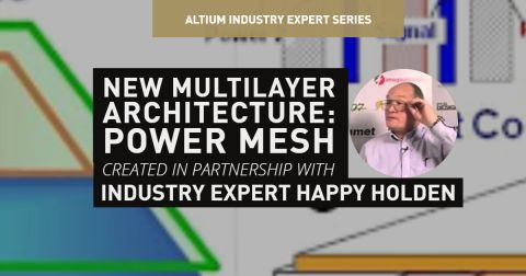
New Multilayer Architecture: Power Mesh
It’s funny how we accept the status quo as the only reality because it’s the only existence we’ve been subject to. In printed circuit design, the multilayer architecture is one such status quo. But it is not the only architecture that will work for high-speed designs. At Hewlett-Packard, we experimented with and implemented a higher performance architecture based on RF Design characteristics. It was not by accident, as our PCB design organization
Read Article
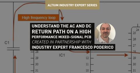
Understand the AC and DC Return Path on a High-Performance Mixed-Signal PCB
High performance mixed-signal PCBs are difficult to design. Proper grounding and routing are essential to ensure accurate ADC conversion. In this article we’ll discuss a complex topic; the importance of designing a controlled current path on high performance mixed (Analog/Digital) PCBs, and how this impacts the performance of your board. What are we going to learn? • Loop currents follow different path (depends from their frequency range.) • How
Read Article
SMTA for Young Professionals
The SMTA is an international non-profit with chapters across the world in the US, Canada, Mexico, India, Europe, Brazil, Hong Kong and Malaysia. Since it’s invention in the 1960’s; Surface Mount Technology has helped reduce waste, reduce consumer costs, and most importantly, reduce environmental impact. This industry is creative and inventive. Everything we touch has been engineered. Our industry leaders shape the world around us. Our goal as an
Read Article
It’s All Analog
“It’s all analog!” I would state emphatically, often banging the table for effect. Those in the room that knew me would continue working, those that didn’t believe me could be seen to roll their eyes, but sometimes I would get the attention of a new hire or someone just out of school, and they might ask “what about digital?” The time was the middle of the 1980s, and I was working at Commodore Business Systems as a senior design engineer, which
Read Article
Insertion Loss Deviation or Intersymbol Interference Noise?
In a previous blog, I discussed how channel quality is quantified by eye patterns [1]. There, it is explained how eye patterns are created from the thru S-parameters only. So, if you are using the thru S-parameters alone, do reflections even matter? Intuitively, it would seem like they don’t matter since they are not directly used to calculate the eye pattern. S-Parameters Still Matter But, of course reflections matter! Reflections cause signal
Read Article
Custom Footprint Creation in Altium Designer
Read Article
Pagination
First page
« First
Previous page
‹ Previous
…
Page
219
Page
220
Page
221
Page
222
Current page
223
Page
224
Page
225
Page
226
Page
227
…
Page
230
Page
240
Page
250
Page
260
Page
270
Page
280
Page
290
Page
300
Page
310
Page
320
Page
420
Next page
Next ›
Last page
Last »
Subscribe to