Skip to main content
Mobile menu
Discover
Develop
Agile
Resources & Support
Free Altium 365 Tools
Gerber Compare
Online PCB Viewer
Resources & Support
Learning Hub
Support Center
Documentation
Webinars
Altium Community
Forum
Bug Crunch
Ideas
Education
Student Lab
Educator Center
Altium Education Curriculum
Search Open
Search
Search Close
Sign In
Main menu
Home
PCB Design
Collaboration
Component Creation
Data Management
Design Outputs
ECAD/MCAD
HDI Design
High Speed Design
Multi-Board
PCB Layout
PCB Routing
PCB Supply Chain
Power Integrity
RF Design
Rigid Flex
Schematic Capture
Signal Integrity
Simulation
Software
Develop
Discover
Agile
Altium 365
Altium Designer
Education
Programs
Altium Academy
Engineering News
Guide Books
Newsletters
Podcasts
Projects
Training Courses
Webinars
Whitepapers
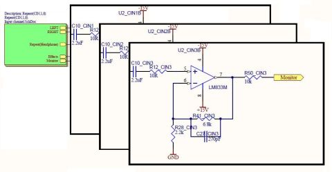
More than a Right-Click Menu Multi-Channel PCB Design
When it comes to creating a schematic I want the tools to work for me and not the other way around. I want easy access to, I want to place and connect those, and I want to be able to do all of this without having to jump through a lot of hoops to get there. Sadly many PCB design CAD systems don’t seem to share my opinion. I’m looking for an easy right-click menu solution while most CAD systems appear to want me to memorize a of ancient texts and
Read Article
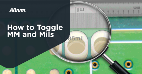
Switching Units From MM to Mils and Other PCB Design Measurement Preferences
Your PCB layout needs to be an accurate reflection of your final design and should follow a specified unit scale. Inside Altium Designer, there are simple ways to set units as you work on the PCB layout, as well as in the schematic where circuits are being created. The short guide below shows how to switch from mm to mil in the Schematic Editor and in the PCB Editor. Users can do this live (while working on the PCB layout) or from the Preferences
Read Article
From Veteran PCB Designers to Next Gen Innovators - July 2018
OnTrack Newsletter July 2018 VOL. 2 No 4 Welcome to the July edition of the Altium OnTrack Newsletter! In Rock Stars and Superheroes, we talk with veteran PCB Designer Bill Brooks, who has been designing boards since 1969. In Next Gen Designers, we introduce you to the WARR Hyperloop team from the Technical University of Munich, who won the SpaceX Hyperloop Pod Competition II in 2017, and broke the world record as well! In the OnTrack video
Read Article
BOM Management Tools for PCB Manufacturing
Between the mid-1980s and late 1990s, Spy magazine published a monthly “Separated at Birth” column/pictorial that would pair two selected photos of unrelated celebrities, cartoon characters, or movie characters. The authors would then point out similar physical characteristics from each photo. Mentally picture a space alien from a popular movie paired with a sultry singer to gain some appreciation for their humor. Separated at Birth? Well… Kinda
Read Article
PCB Material Selection: How Substrate Properties Impact PCB Performance
From the early 15th century until the 17th century, artists used the Flemish masters’ method to create life-like paintings. This process begins with a pencil, charcoal, or ink pen drawing and continues with the imprimatura—or the first transparent, olive-tinged stain of color. Then, the method moves to the first umber underpainting, sanding, second umber underpainting, sanding, and a monochromatic underpainting. Each underpainting layer focuses
Read Article
How to Avoid PCB Component Failures and Workaround Them
Probably, the single thing that drew me to pursue a technical career was the existence of laws that stipulated if you follow the same procedure then you will get the same results. I have always taken comfort in having that security for my work. However, there is another law that at times supersedes all others. That, of course, is Murphy’s law, which states “Anything that can go wrong will go wrong.” At times it seems that Murphy’s law applies
Read Article
Escape the Pain of a Gerber Files Viewer and Invest in a 3D PCB Editor
As the design of printed circuit boards grows more challenging with flex, rigid-flex, RF, and other technologies, it is becoming more important than ever to be able to see exactly what it is that you are designing. Then compounded by shorter design cycles and fewer prototype builds the need for full verification of the design before manufacturing has become a necessity. Thankfully PCB design tools have kept pace with different ways to view and
Read Article
Annotate Reference Designators With Custom Global Properties
Having a system to find many similar items in a short amount of time can be helpful in staying organized. Everybody has a silverware drawer and most are organized with caddys that divide the flatware into forks, knives, and spoons. Reference designators are the unique identifiers on a PCB for each and every component or free pad on the design. Best design practice is to number the reference designators consecutively on the PCB to allow easy
Read Article
41
Unlimited Mechanical Layers - Sneak Preview
Watch Video
What's New In Altium Designer Webinar July 24
Altium Webinar: July 24th In case you missed our Altium Designer
®
live webinar, no worries. You can catch up here with the video recording and presentation slides. If you’re not a fan of videos I’ll try my best to summarize in the webinar notes below. Most of the key takeaways will be the same as the may webinar but do take a look at the questions as they’ll be different. For future webinars, if there’s something you’d like to see add it to the
Read Article
Pagination
First page
« First
Previous page
‹ Previous
…
Page
274
Page
275
Page
276
Page
277
Current page
278
Page
279
Page
280
Page
281
Page
282
…
Page
290
Page
300
Page
310
Page
320
Page
330
Page
340
Page
350
Page
360
Page
370
Page
380
Next page
Next ›
Last page
Last »
Subscribe to