Skip to main content
Mobile menu
Discover
Develop
Agile
Resources & Support
Free Altium 365 Tools
Gerber Compare
Online PCB Viewer
Resources & Support
Learning Hub
Support Center
Documentation
Webinars
Altium Community
Forum
Bug Crunch
Ideas
Education
Student Lab
Educator Center
Altium Education Curriculum
Search Open
Search
Search Close
Sign In
Main menu
Home
PCB Design
Collaboration
Component Creation
Data Management
Design Outputs
ECAD/MCAD
HDI Design
High Speed Design
Multi-Board
PCB Layout
PCB Routing
PCB Supply Chain
Power Integrity
RF Design
Rigid Flex
Schematic Capture
Signal Integrity
Simulation
Software
Develop
Discover
Agile
Altium 365
Altium Designer
Education
Programs
Altium Academy
Engineering News
Guide Books
Newsletters
Podcasts
Projects
Training Courses
Webinars
Whitepapers
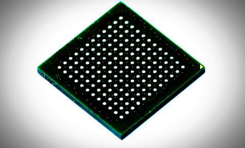
Avoid Signal Integrity Loss While Using a Fanout Strategy in Your PCB
When I was much, much younger, I looked at the pin layout on the back of a processor and wondered how anyone can possibly route all of those electrical connections on a PCB. I didn’t know much about signal integrity, of fanouts on PCBs then but fast forward fifteen years and now I get to layout those traces on PCBs. Fanout is a technique where short traces and vias are used to connect inner rows of pins on high pin-count ICs. Fanout can also
Read Article
Coatings vs Resins for Your PCB: What’s Best for Providing Protection?
In today’s world, protection is always a welcome asset. Whether it be protection from the rain above your head (mitigated by a roof), protection from the sun (mitigated by sunscreen), or protection from electromagnetic currents (mitigated by current isolation techniques amongst others). With resin and conformal coating for your PCB, you can think about the forces that attack your PCB from a physical (environmental) standpoint - beyond EMI
Read Article
IoT Resources for Developers
From the early days of printed circuit boards, the electronics industry has made huge strides in board materials, copper printing methods, miniaturization, rigid-flex, ELIC, EDA, and much more. Many of the devices we use in our homes, our vehicles, and in our workplaces would not be possible without this continuous evolution of PCB design and technology. The scope of creativity from individuals is unbounded. While the infrastructure for IoT can
Read Article
Schematic Capture Considerations
Become an expert PCB Designer when you use Altium Designer software and master schematic capture. Benefits to the Unified Data Model Approach include not just time savings, but the potential of the Unified Data Model Approach is limitless. Consider the big picture and the very details that impact your projects' success. Click the PDF above to read more about schematic design in this presentation overview. Or view the original content here: High
Read Article
How to Simplify PCB Design
Become an expert PCB Designer when you use Altium Designer software. Benefits to the Unified Data Model Approach include not just time savings, but the potential of the Unified Data Model Approach is limitless. Consider the big picture and the very details that impact your projects' success. Click the PDF above to read more about How to Simplify PCB Design in this presentation overview. Or view the original content here: How to Simplify and
Read Article
2:13
Release Management
Watch Video
1:20
MCAD Integration
Watch Video
1:51
Panelization
Watch Video
Learning the PCB Design Software Shortcuts to Hack Your Design Growth
Even simple PCB designs can require the use of many functions and tools, and this doesn’t change if you’ve been a designer for 20-minutes or 20-years. One feature that will always make your PCB design software more efficient is using keyboard shortcuts. So how can you improve your efficiency beyond where it's at now? With a little help from Altium Designer and the shortcuts they’ve so graciously added to the program! No matter how quick your
Read Article
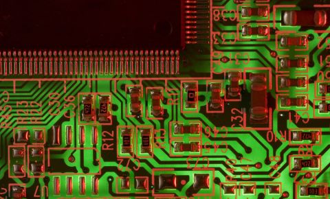
Routers in PCB Boards: Working with Altium Designer’s Multilayered Via Routing Rules
Some of the first ideas and drawings of two-layered PCB design came at the turn of the century, right before the world would descend into its first world war. It should come as a surprise that an idea and an adaptation to circuit boards, two-layers, developed over one-hundred years ago is still alive and well. But it should come as no surprise that with time comes new adaptations, and the era of multilayered stackups is much more appropriate for
Read Article
Pagination
First page
« First
Previous page
‹ Previous
…
Page
291
Page
292
Page
293
Page
294
Current page
295
Page
296
Page
297
Page
298
Page
299
…
Page
300
Page
310
Page
320
Page
330
Page
340
Page
350
Page
360
Page
370
Page
380
Page
390
Next page
Next ›
Last page
Last »
Subscribe to