Skip to main content
Mobile menu
Discover
Develop
Agile
Resources & Support
Free Altium 365 Tools
Gerber Compare
Online PCB Viewer
Resources & Support
Learning Hub
Support Center
Documentation
Webinars
Altium Community
Forum
Bug Crunch
Ideas
Education
Student Lab
Educator Center
Altium Education Curriculum
Search Open
Search
Search Close
Sign In
Main menu
Home
PCB Design
Collaboration
Component Creation
Data Management
Design Outputs
ECAD/MCAD
HDI Design
High Speed Design
Multi-Board
PCB Layout
PCB Routing
PCB Supply Chain
Power Integrity
RF Design
Rigid Flex
Schematic Capture
Signal Integrity
Simulation
Software
Develop
Discover
Agile
Altium 365
Altium Designer
Education
Programs
Altium Academy
Engineering News
Guide Books
Newsletters
Podcasts
Projects
Training Courses
Webinars
Whitepapers
PCB Design Career and Team Tips Presentation
Become an expert PCB Designer when you use Altium Designer software. Benefits to the Unified Data Model Approach include not just time savings, but the potential of the Unified Data Model Approach is limitless. Consider the big picture and the very details that impact your projects' success. Click the PDF above to read more about PCB Design Career & Team in this presentation overview. Or view the original content here: How to Become a PCB
Read Article
Model Copper Roughness Properly, a Discussion with Bert Simonovich
Discover how to model copper roughness properly with insights from industry expert, Bert Simonovich. Nail down your design to achieve consistent result. Listen to this podcast episode to learn more.
Read Article
Keep Your Altium Designer PCB Layout in Line with Grids and Grid-Selection Shortcuts
The grid system in a printed circuit board design CAD program is a great tool for a PCB designer, and it's a system worth knowing. Altium Designer
®
has a well designed grid system that you can use to your advantage in your PCB designs and schematic captures. Before all the different snap and placement utilities that are now available in CAD systems, we used to have to constantly manipulate the grid to place objects at different locations. It
Read Article
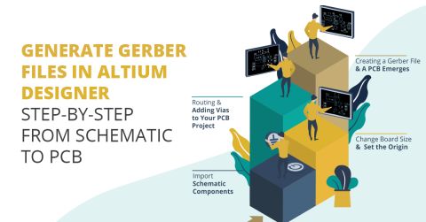
How to Make PCB Gerber Files in Altium Designer Step-by-Step
Looking for the best approach for CAM jobs? Learn how to make PCB Gerber files in Altium Designer from your circuit board layout. Altium's CAM tools can help you quickly create PCB Gerber files.
Read Article
GPS Antennas in Your PCB Design: You Won’t Get Lost Again
Going on hunting trips with my grandpa as a kid, we would carry a rather large GPS-navigator to help us keep from getting lost in the woods. It had a huge antenna sticking out the top and its battery never lasted longer than a few hours. Fast forward 20 years, and including GPS capabilities in your PCB design has become easier than ever. Many new consumer devices include GPS PCB antenna modules in their design. If you don’t have GPS or RF-design
Read Article
Dual-Band PCB Antenna Design: Keeping Your EMI In-Line
If you were born in the 1980’s or earlier, you probably remember those old brick-like cell phones and their giant antennas. Fast forward to the present, and most people don’t even realize that their smartphones have antennas. Proposed antenna designs have come a long way since the 80’s, and new antennas can send and receive in more than one frequency band. As the mobile and IoT industry continues to advance, electronic devices continue to use
Read Article
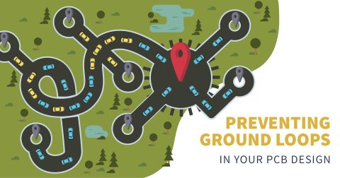
Preventing Ground Loops in Your PCB Design
I think we’ve all been there. You buy that awesome stereo system only to hear that familiar humming sound in the background. When you take it back to the store the clerk blames the manufacturer. What components are to be considered a problem? The decoupling capacitor or ground wire? How about the bypass capacitor or PCB ground loop design interference? The stereo manufacturer will blame the component manufacturer and the component manufacturer
Read Article
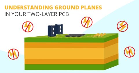
Understanding 2-Layer PCB Ground Planes
Like many designers, my first board was a 2-layer board, and it didn't use a PCB ground plane. It wasn't very elaborate, just an amplifier with some connectors and a connection to a DAQ module that interfaced with a LabVIEW app. When you're designing with through-hole components on a copper-clad perfboard, there's no way to create a solid ground region anywhere on the board, and your grounding strategy will suffer for it. If you watch the
Read Article
How to Read PCB Assembly Drawings
Here is a complete list of information PCB designers can get from a PCB assembly drawing. This information helps with design re-spins or rework, as well as mechanical design.
Read Article
Introduction of 3D Technology in PCBs: 3D Printing and PCB Design
Early experimental jets from the design table to wind tunnel tests of models to actual piloted flight at a rapid rate. During the 1950s, aircraft designers relied on slide rules and blackboard mathematics rather than computer processing and virtual simulations. When a test pilot climbed into a cockpit, he climbed into an untested prototype. Some flights went very well and set speed and altitude records, while other flights… didn’t. As with
Read Article
Pagination
First page
« First
Previous page
‹ Previous
…
Page
293
Page
294
Page
295
Page
296
Current page
297
Page
298
Page
299
Page
300
Page
301
…
Page
310
Page
320
Page
330
Page
340
Page
350
Page
360
Page
370
Page
380
Page
390
Page
400
Next page
Next ›
Last page
Last »
Subscribe to