


100A 12V H-Bridge Project

At a Glance
Synopsis: Build a powerful 1200W motor driver with Mark Harris in this open source H-Bridge project. Learn about H-Bridges, and designing high current circuit boards with this 100 amp demonstration board.


What is an H-Bridge circuit and where can they be found? The H-Bridge circuit forms the basis of many power electronics projects such as motor drivers, inverters, and large switching power supplies. Read this extensive article which guides you through the design process of building your own H-Bridge project:
—
This article will be taking you through the design process of a 100A capable H-Bridge project. We’ll discuss the challenges of working with very large currents, as well as the implementation of the H-Bridge and its driver. This board could be used for motor driving, as it is designed for powering a 12V winch motor, or as the foundation for your own project implementation. H-Bridge circuits form the core of many power electronics projects, such as motor drivers, inverters, and large switching power supplies.

As always, this project is completely open source under the MIT license which allows you to freely use any part of the design for any application commercial or otherwise. You can find the Altium Designer project files for the project hosted at GitHub.
What is a H-Bridge?
An H-bridge is a versatile circuit that has numerous applications in power electronics. In our case for this project, it is being used as a brushed motor driver. It is also commonly used in DC to AC inverters, such as those in an Uninterrupted Power Supply (UPS), high power DC/DC converters and all types of motor drivers including 3 phase and stepper motor drives.
It gets its name from the typical schematic representation of the circuit, forming a letter H with the load in the center as shown below. For switches (N-Channel MOSFETS in the example below) allow current to flow from VCC to GND through the load (J1 below) in either direction. For brushed DC motors, this allows bidirectional motor control, and if the two high sides or low sides are both on at the same time, the motor can have a braking action applied. If IC1 and IC4 are enabled, the motor would go in one direction, and if IC2 and IC3 were enabled it would turn the opposite direction. Driving the MOSFETs with a PWM signal, speed control can be easily accomplished.

A critical failure mode of an H-bridge is when both switches on one side of the load are switched on at the same time, an event called a shoot-through. For example, if IC1 and IC3 were on at the same time. In the event this were to happen, a direct short would be created from VCC to GND - this would be a very bad thing.
To avoid bad things such as this happening, H-bridges are almost always controlled with some intelligent logic, either from a microcontroller or an H-bridge driver - or better yet, a microcontroller connected to an H-bridge driver. Not all H-bridge drivers have shoot through protection, and specialized H-bridges may be built using individual drivers or multiple high/low drivers that only control one side of the bridge each. Even with a driver that has shoot through protection built in, a shoot through event is still very possible if the protection is misconfigured.
The H-Bridge Driver
In this project we’re going to utilize the Renesas HIP4081A high frequency full bridge FET driver. I’ve used this driver extensively in the past with great success and currently it's one of only a small handful of full bridge drivers that were in stock for my prototyping needs. The HIP4081A is likely to be around for a long time, as it comes from a long heritage of drop-in replacement bridge drivers with a history that spans over 20 years. If it stops being manufactured, I'm fairly confident there will be another drop in replacement component available to replace it. It's going to take care of the vast majority of the bridge driving for us, and keep things safe in the process.

H-bridge drivers excel at a number of critical functions where a microcontroller would need substantial additional circuitry:
Bootstrapping a high voltage for N-Channel high side MOSFETS.
Providing sufficient voltage to ensure each MOSFETs reaches minimum Rds(on).
Rapidly switching MOSFET gates on and off.
Managing dead times to prevent a shoot-through condition.
Depending on the application of the H-bridge, the driver may need to switch the MOSFETs on and off relatively fast, DC servos being a use in the past where I’ve driven an H-bridge at up to 1MHz. It may not sound like much in the grand scheme of things, however remember that each time you turn the FET on, you need to charge the gate, and then to get the FET to switch off completely you need to drain the charge in the gate. Small gate charges can quickly add up to several amps of drive current being required.

To this end, we are going to implement a low value resistor and diode on each gate output of the driver. The resistor will act to limit current to the MOSFET gate, but only enough to ensure the driver does not burn out. Many high current rated MOSFETs have large gate capacitance which can cause substantial inrush current. The diodes allow the gate driver to drain the charge from the gate as rapidly as possible, ensuring the MOSFET is completely switched off before its counterpart switches on.
To generate the high side gate voltage, the driver uses a fairly typical charge pump to bootstrap the voltage.

The diode allows 12v to the boost pin, with the capacitor referenced to the source of the high side MOSFET.

The dead time delay is configurable using resistors on the HDEL and LDEL pins, typically you would use a 200k potentiometer on these pins to start at the maximum resistance, and then using your oscilloscope to monitor the gate voltage, bring the delay down until the delay is approaching the gate being drained without getting too close. You need to ensure there is a safety buffer in the timings to account for tolerances and variations in components across a production run. I’ve found for my uses that 75kOhm provides a sufficient delay, however this is not guaranteed to be appropriate for your application.
H-Bridge Design
With the driver schematic complete, we can start looking at the H-bridge itself. This H-bridge is being designed to run on a regular car battery to drive a winch motor - nominally this is a 12v supply however the state of charge will vary that considerably. Our H-bridge design has quite a few extra components compared to the bare bones example earlier in this article.
I’ll cover the basics of my design choices in this article, however if you want to read my in depth guide on every technical parameter relevant to designing your own H-Bridge, be sure to check out my Making Big Brushed Motors Move article over at Octopart.

The most critical additional components in the full implementation of the H-bridge are the MOSFET protection diodes. The flyback voltages generated by an inductive load such as a DC motor will destroy the MOSFET’s body diode within the first few activations of the H-bridge, if they don’t fry on the first use. For the protection diodes I’ve selected low forward drop diodes with a decent current rating.
I’ve also added current sense resistors to the bridge. While they are not necessary for operation, they do allow for some interesting control options when paired with a microcontroller. I’m using two current sense resistors per leg in parallel as the current density around and dissipation through a single resistor is just too high.
There is also an RC snubber across the motor connections, to help suppress voltage spikes. Additionally, there are two LEDs to indicate the direction the H-bridge is being driven - you can never have too many indicating LEDs!
The motor is connected through a massive connector, a Molex 0399200302 rated for 115A of current. With a 15mm pitch, it can take 1-8AWG wires and sits 1.38”/35mm high. On the circuit board, it slightly warps your perception of scale if you’re used to dealing with 0.1”/2.54mm pitch connectors.
But wait, there’s more! The MOSFETs I’m using are rated for 150A, but there is no way we can actually feed that current through their small footprint so I’m doubling up the MOSFETs. If this was a high reliability H-bridge or was going to see elevated service temperatures I’d add a third or even fourth set of MOSFETs to the bridge, or just change out the MOSFET for a much larger package.

I chose these MOSFETs as they had the lowest Rds(on) of any stocked MOSFET at the time of design, while having a relatively decent thermal package and most importantly, after on-resistance, they had low gate charge/capacitance parameters. Even having two or three in parallel these MOSFETs still have acceptable gate parameters for this circuit.
Controlling the H-Bridge
This project board does not contain a microcontroller, instead it features a couple of buttons and an external header allowing for control input from the source of your choice. As I have both onboard buttons and external inputs I have added a bit of additional circuitry to ensure everything works as expected no matter the input source.

First off, we have our enable/disable switch for the H-bridge driver. The driver has an active high enable input, so high is on, low is off. This will either pull the enable pin up or down, with the resistor R14 limiting current. If the enable switch is set to 3.3V and the external input is set to GND, we want to ensure that current is limited so there is no short circuit. An external driver that is an open drain would be ideal, as the enable pin would still function as expected on the H-bridge board allowing the driver to be placed into a disabled state if need be.

Both the buttons on the board have the same implementation, effectively creating forward/reverse buttons for the motor. The HIP4081A’s low side inputs take precedence over the high inputs, so if we just wanted to have button input we could easily pull the AHI/BHI pins high and simply control the ALI/BLI pins. Without knowing the input controls however, I’m going to use a hex inverter IC for ensuring ALI is always the inverse of AHI and the same for channel B.
In the schematic above, R16 is set as a Not Fitted variation for this board. I have selected a push-pull inverter, however if an open drain inverter were to be used, the pull up would be required.
PCB Layout
Before starting any layout or routing for this project, we have a bit of setup to do first. With 100A coursing across the board, we can be certain that heavy copper and a 4 layer board are going to be critical to the project’s success.

The first thing I’m setting up is a 4 layer board with 70μm/2oz copper on the outer layers, this is a fairly minor cost increase with most board manufacturers. Keeping the internal layers at 17.5μm/0.5oz will also keep costs down, and give us somewhere for less power critical nets. I’m not modifying the dielectric constant of the board, this is definitely not an impedance matched board, as most of the critical routing will be done with polygons!
After setting up typical design rules, it’s time to start creating a rough layout. One non-typical design rule I needed to change was for component height, as those Molex connectors are too tall for the default rule.
Driver Layout
I’m starting the board with the driver layout, as it has the most components to arrange.

Initially I’m just positioning the core components for the functionality of the H-bridge - the capacitors, bootstrap components and delay resistors. There are also the gate drivers, but I wanted to see how the H-bridge would come together before deciding exactly where they would go.

I ended up deciding to place the gate driver components against the driver IC to keep as much copper around the MOSFETs as possible for thermal and current capacity.
H-Bridge Layout

When grouping all the components for the H-Bridge together, it’s immediately apparent that the connector dwarfs everything else for the H-Bridge - so we’ll start by building the H-Bridge around it.

My initial layout is fairly compact, I tried placing the MOSFETs on the left and right sides of the connectors but ended up deciding to create a flow from top to bottom on the board. Things are pretty closely spaced together, so this layout will almost certainly change as the design progresses.

To help with determining where other components can be placed on the board, I’m using a silkscreen box that is 25mm square to create a boundary area round the outermost MOSFETs. The datasheet for the MOSFETs suggests a 25mm2 area for heat sinking on 70um copper boards, so I’ll be ensuring there is at least this much copper around the MOSFETs.

Needing spacing for thermal reasons led to increasing the distance between the MOSFETs and the current sense resistors, as well as between the MOSFETs and motor connector.

I used the thermal courtyard around the MOSFETs to help determine the location of the power input connector. I’m trying to keep it relatively centered on the motor connector to balance the thermals/current on each side of the bridge.

With a block of silkscreen on each MOSFET, all the additional components for the H-bridge have been positioned - giving a much firmer idea of how large the board will be.

In addition to the Molex connector for connecting wires to the H-bridge, I’m also adding holes for M6 bolts. The ring for the hole is the same size as a M6 washer to ensure good contact. The idea for these holes is to allow the connection of large wires with a ring terminal on the end, such as my winch motor has. Using a brass or copper bolt with similar washes, a low resistance connection can easily be made to the board.
Controls Layout
With the H-bridge and driver having gone through a first pass layout, I have an idea of what board space remains for our controls and off board connections. I’m trying to keep the controls close to the driver, so that the board sees minimum disruption from the traces between the controls and the driver.

Finalizing First Pass Layout
All the components are now in a location that I’m happy with, though these may not be the final locations. It is very easy to get a components location stuck in your head as the final place it will be - but nothing should be considered final until the board is signed off for production.

You might also notice all the test points are still off board, these will be the last items we add to this board. Personally, I prefer placing test points on a via where there is a layer change, this keeps the impedance change on the trace all in one place and also gives a nice registration to a pogo pin. With this in mind, I won’t know where they will be going until we have the routing completed, or mostly completed.
Starting Routing
I’m going to start routing the H-bridge first, getting the large polygon pours in place before we look at any of the low current signals. Having the large, critical copper areas well defined will let me determine where the other tracks will be able to run.

I’m using my previous layout guidelines on the top overlay layer to determine the size of the polygon pours. I’ll also have these polygons mirrored on the bottom layer for added thermal mass and conductor area.

The first pass of the polygon layout is completed, the vias are definitely not going to be final - they are mostly there to see what happens during simulation. One thing I haven’t accounted for at this point of the layout is that the 12V net has substantially more copper area feeding it than the GND net. With the current sense resistors breaking the GND of the H-bridge it leads to an unbalanced supply copper. We’ll have to see what happens during simulation and then modify the layout as needed.
Routing the Driver
The driver is pretty simple to route, other than a few considerations around the gate nets. The gate pins could be carrying up to 0.5A with the MOSFETs in this design, however this could be significantly higher with other MOSFETs or additional MOSFETs in parallel.

To maximize copper area around the MOSFETs, I’m trying to place the gate net as close to the MOSFET as possible, despite the relatively large via.

With the inner copper layer being just a quarter of the cross sectional area of the outer layers, I’m using much larger tracks on the internal layers. While there isn’t much else going on this mid layer, the vias we’ll need for thermal and current carrying do substantially reduce the amount of area available for tracks - therefore, this 2.5mm track is about as large as I can reasonably fit.

After adding the final nets for the driver and controls, and adding polygons to make the internal layers mostly ground, the board is ready for PDN Analyzer simulation. I’m only going to be simulating the H-bridge, as the current on the driver nets are not high enough to be of any concern.
PDN Analyzer
For any moderate current or above design I always recommend doing at least some simulation or calculations on the copper area. The simulations can immediately highlight obvious goofs and quickly offer insight into whether the board will survive testing. It's all too common when dealing with tens or hundreds of amps to feel as though the huge swaths of copper you have are sufficient, only to find the current densities are very high in some areas - and risk the success of the whole project.
Simulation Resources
I’m not going to cover the PDN Analyzer setup in this article, if you’re interested in how to setup a PDN Analyzer simulation take a look at my PDN Analyzer quick start guide. The quick start guide runs you through the setup of a much lower current single chip motor driver. You might also find my PDN Analyzer simulation of a 65W LED driver interesting too. If you’re stuck trying to figure out if your output is meaningful, I have an article on copper current density which can help make sense of the simulation results.
Initial Simulation Results
I have my simulation setup so the A side (right) of the H-bridge is our high side, with the B side being ground. This leaves the bottom right corner unused, so I’ll just be mirroring the bottom left corner for its layout changes.

With a current density limit of 100A/mm2 set, anything over that will show up as black. We definitely have some hot spots here that we can greatly improve. I expect the area under the MOSFET drain/source pins and the current sense resistor pins will be impossible to bring down - it’s just a matter of maximizing the ability for current to get to and from those pins.
Optimizing the Layout
One of the most immediate issues which is easy to resolve is the current sense resistors. These are both jammed into a corner of the copper area and very close together - this not only increases the amount of current moving through the local area, but also the path between the MOSFETs and the resistors is getting fairly saturated as well. Additionally, this is not ideal thermally for the current sense resistors as we are bringing all the heat they generate into a very small area of the board.

The first change I’m making is to get the resistors out of the corner, and spread them across the polygon area.

Next I’m moving all the MOSFETs apart as well, a little extra spacing should help reduce the current density around their drain/source pins.

For the second simulation run, I have no vias at all. Overall, the current density around the MOSFETs and resistors is dramatically lower. The copper area is also being better utilized for current carrying - the current density with just the top layer is now about the same as with multiple layers carrying the load.
With just the top layer carrying current however, the ground polygon is fairly dire. The necked down area of ground just can’t cope with 100A flowing through it.

Just adding vias to the GND polygon has greatly improved the situation, however I also have the inner layer polygons shelved which, while much thinner copper than the outer layers, will carry some of the current burden.

Just unshelving the inner layer polygons removed the area in the neck that was still over 100A/mm2. The current density is still really high - but we’ll get to that a bit later. First we need to add vias to the other polygons to see if we can bring the current density down a little for those nets.

I’ll admit, I had far too much fun adding vias to the other polygons and may have gotten a little carried away. The current density shows dramatic improvement however, especially in the upper polygons where you have the through hole connector. The through hole connector enables very effective use of the top and bottom layers for carrying current. We still have very high peak current density under the MOSFET drain and source pins, as well as the resistors, however, it is almost entirely localized to just the area of the pads themselves.
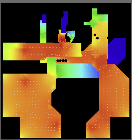
The above screenshots have been taken with a maximum current density limit of 100A/mm2, and minimum of 0A/mm2. Changing this to a minimum current density of 2A/mm2 shows a much more revealing picture of the board.

When the colors transition from blue to black, the current density is under 2A/mm2, and from red to black, the current density exceeds 100A/mm2. With the H-bridge moved away from the bottom edge of the board, the current density is greatly reduced through the necked down area. This color gradient might be less meaningful for a report however for optimizing the layout it clearly reveals the areas of high current flow, and what copper is perhaps somewhat wasted for current carrying.

Changing the minimum current density up to 10A/mm2, it makes the simulation even cleaner. For my designs I prefer to stay under 30A/mm2 in general, and we can see that lines up fairly well with green. Other than very localized areas of high density around the MOSFETs, connector pins and current sense resistors, the H-bridge is mostly under my personal arbitrary limit.
With this simulation result, I have the confidence that the board will perform substantially better than the initial layout in the real world, and will have far less worries about overheating or blown copper.
Can PDN Analyzer help you optimize and sanity check your own hardware? Talk to a PDNA expert today to find out more.
One final optimization to make is the corner on the 12V net against HIGHSRC_B - it’s a localized high density point, which I previously cleaned up on the GND side of the bridge. Just adding a simple chamfer to that corner will clean it up.

In the regular PCB view, this is how the polygons now look with the vias. As I said before, I got a little carried away with placing vias - I was having too much fun. Halving the number of vias in the bridge would have very little impact on the current density, however I do like redundancy! The vias reduced the peak current on the copper between the connector pins/MOSFETs and MOSFETS/resistors by about 50-60A/mm2, so the vias are carrying some current, though the top of the board remains the primary conductor.
Altium Designer’s integrated simulation tools paired with industry leading schematic capture and layout tools help me rapidly develop optimal hardware solutions with the least amount of effort. Talk to an expert at Altium to find out how Altium Designer can accelerate your next project.
About Author
Related Resources
Related Technical Documentation
Design to Release, Without the Friction
- Keep reviews tied to the right version
- Reduce handoff confusion and rework
- Spot sourcing and release risk earlier
- Work solo, share when needed
Get Started
Thank you, you are now subscribed to updates.