
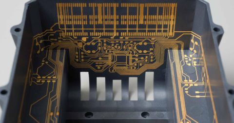


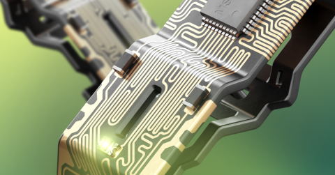


What Is Printed Electronics Design?

At a Glance
Learn how printed electronics differ from PCB design, from materials to manufacturing. Explore key design challenges, methods, and future innovations.


The answer is simple: it is electronics design. It involves applying circuit theories, mathematical calculations, and computer-based simulations to design electrical functionality and performance using printed electronics materials.
How Is Printed Electronics Different From Traditional PCB Design?
Materials are the key factor in printed electronics, as they have different electrical performance characteristics compared to those used in traditional PCBs. Additionally, the construction methods for printed electronics differ from conventional PCB manufacturing.
In traditional PCB design, the process for creating traces is well established. First, an electronics engineer designs the circuit, defines its dimensions based on electrical requirements, and, once finalized, generates the necessary manufacturing files.
During manufacturing, the PCB is produced according to these design files by transferring electrical circuits onto a copper layer. For example, a masked UV-sensitive photoresist film is exposed to UV light, and the unexposed copper is then etched away, leaving behind the designed traces. These traces meet the required dimensions and electrical specifications.
In printed electronics, the goal is the same—to create functional circuits that meet electrical requirements—but achieving this requires different design rules, materials, and manufacturing processes.
The Inputs and Outputs of Printed Electronics Design
The inputs and outputs of printed electronics design are essentially the same as those in PCB design. The key factor between input and output remains the same: electronics design. You must incorporate material properties and design rules into the process, with the final output being manufacturing files.
The same physical laws apply to both PCB and printed electronics design, defining the boundaries of what can be achieved. Two circuits—one made using traditional PCB methods and the other using printed electronics—can perform the same function, yet their designs will differ. This is due to the physical capabilities and limitations of the materials used in each type of circuit.
In both cases, voltage differences must be applied across impedance to generate current flow. Achieving the same current in both circuits requires either matching impedance levels or adjusting circuit-specific voltage settings. In printed electronics design, these parameters are carefully adjusted to find the optimal balance by fine-tuning impedance and setting the correct voltage levels.
Understanding Material Characteristics in Printed Electronics
In electronics design, understanding the material characteristics of the final product is essential. In PCB design, key parameters include copper thickness, sheet resistance, thermal properties, and the dielectric constant of the PCB material. The same parameters must be considered in printed electronics. For example, what is the final thickness of the silver ink conductor? What is its square resistance? What is the dielectric constant of the substrate material?
Electronics design must account for these new materials. Ohm’s Law, Kirchhoff’s circuit laws, and Maxwell’s equations apply to printed electronics just as they do to traditional PCBs.
There are hundreds of different conductive inks available, each with unique square resistivity. Some inks offer high conductivity (though still lower than pure copper), but after curing, they become rigid and cannot elongate. Others remain stretchable after curing but have significantly lower conductivity. In printed electronics design, it is crucial to understand the square resistance of the chosen ink after final curing to ensure optimal circuit performance.
The Impact of Manufacturing on Design
Another design challenge in printed electronics is that material parameters depend on the production process. The method used to print conductive inks, the curing process, and the presence of other printed inks beneath the conductor all impact the final square resistance.
If the production process changes, the layout design may also need to be adjusted. Alternatively, the production process must be tailored to meet the electrical circuit requirements of the design. It is crucial to have a deep understanding of printed electronics manufacturing.
In PCB manufacturing, designers must also understand how boards are built and the limitations of a specific production process. However, PCB manufacturing methods are more standardized, with only slight variations in capabilities between manufacturers. In contrast, printed electronics manufacturing is not yet at this level of standardization.
Printing Methods for Conductive Inks
Conductive inks can be printed using several methods, with screen printing and inkjet printing being the most common. Many other techniques are also available, which can be explored through further research.
The key aspect of the printing process is understanding both its manufacturing capabilities and limitations. Important factors to consider include:
- What is the minimum clearance required between traces?
- How many conductive layers can be used?
- What are the minimum and maximum trace widths?
It is essential to familiarize yourself with the design rules of the production process you intend to use and ensure your design adheres to them. Many design rules available in PCB design tools can be applied directly to printed electronics, provided they are correctly defined.
However, if the manufacturing process includes design rules not supported by the electronics design tool, manual design rule checks will be necessary. For example, if multiple conductive layers are used and isolated by printed dielectrics, the same design rules apply between the first and second conductive layers as they do for traces on the same layer. Unfortunately, standard PCB design tools do not always support these rules.
Component Assembly in Printed Electronics
Printed electronics also require components for functionality, but assembling components on a printed electronics circuit does not follow a standard soldering process. Since typical printed electronics materials are plastics, their thermal characteristics differ from those of PCBs or flexible printed circuits (FPCs). As a result, different adhesive materials are required.
Low-temperature solders, conductive glues, or other adhesive materials are commonly used in printed electronics surface mount assembly (SMA), and these may require specialized component footprints. Key design considerations include:
- Can traces be routed beneath components?
- Are special keep-out areas needed?
- What types of components are suitable for printed electronics?
These factors must be approached differently compared to standard PCB SMA. Additionally, manufacturing files for surface mount assembly may also differ. For example, can a paste stencil file be used, or is a dispensing glue map required instead? It is essential to verify the specific SMA requirements in advance.
Challenges and Future of Printed Electronics Design
Because printed electronics is a relatively new technology, information on material characteristics and manufacturing methods is not as widely available as it is for PCBs. Additionally, there is a vast range of printed conductive inks, each with different electrical properties. The final characteristics of a printed circuit depend on both the materials used and the specific manufacturing equipment and processes.
Electronics design in this field relies on applying established theories to new materials and manufacturing techniques. In my view, electronics design involves utilizing theories, physics, and mathematics to ensure electrical functionality and performance. This requires a deep understanding of material properties as a fundamental input.
In printed electronics, I have observed a lack of comprehensive material data, leading to decisions made without proper calculations. When design choices are based on guesswork rather than engineering principles, it is no longer true electronics design—it becomes speculation.
Learn More About Printed Electronics with Altium
Would you like to find out more about how Altium can support your printed electronics design?

About Author
Related Resources
Table of Contents
- How Is Printed Electronics Different From Traditional PCB Design?
- The Inputs and Outputs of Printed Electronics Design
- Understanding Material Characteristics in Printed Electronics
- The Impact of Manufacturing on Design
- Printing Methods for Conductive Inks
- Component Assembly in Printed Electronics
- Challenges and Future of Printed Electronics Design
- Learn More About Printed Electronics with Altium
Design to Release, Without the Friction
- Keep reviews tied to the right version
- Reduce handoff confusion and rework
- Spot sourcing and release risk earlier
- Work solo, share when needed
Get Started
Thank you, you are now subscribed to updates.