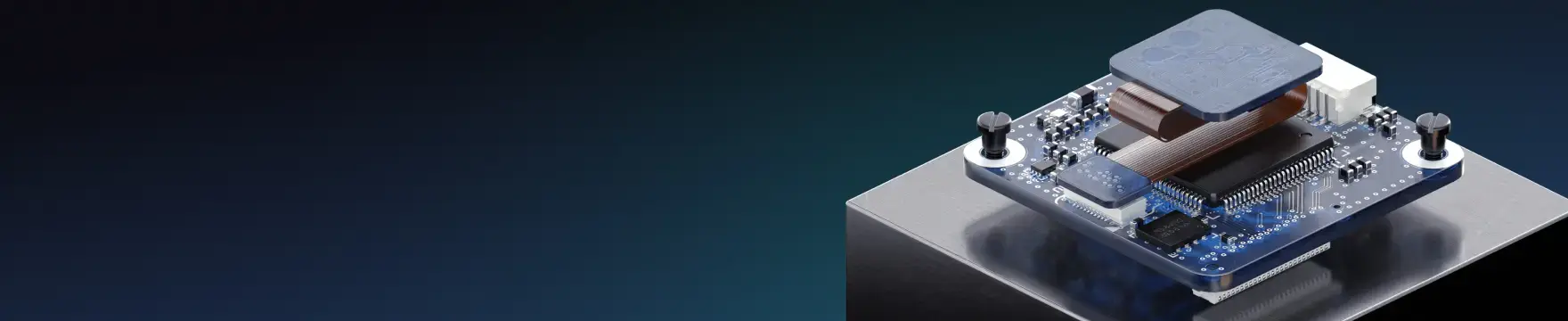


Chiplets and Advanced Packaging: Modular Integration for Next-Generation Electronics

At a Glance
Move past monolithic SoCs. Discover how chiplets and modular integration slash costs and boost performance for next-gen electronics.


The era of "bigger is better" in semiconductor design has officially hit a wall. For decades, Moore’s Law, the observation that the number of transistors on a microchip doubles every two years, was maintained by simply shrinking components. But as we push into 3nm and 2nm territories, we are discovering that traditional monolithic (single-die) systems-on-chip (SoCs) are becoming economically unsustainable. Manufacturing massive, single-die chips at these leading-edge nodes leads to plummeting yields; a single speck of dust can ruin an entire dinner-plate-sized wafer of silicon, making costs astronomical.
The solution isn't just about how many transistors you can cram onto one piece of silicon, but how effectively you can stitch different pieces together. Enter the age of chiplets and advanced packaging, a modular Lego-fication of electronics that is set to democratize high-performance computing.
Key Takeaways
- Chiplets replace large monolithic SoCs. Smaller dies improve yield, reduce cost, and allow mixing different process nodes in one package.
- Advanced packaging (2.5D and 3D) enables high‑density integration. Side‑by‑side interposers and vertical stacking increase performance but introduce major thermal challenges.
- Standardization is essential. Interfaces like UCIe allow chiplets from different vendors to communicate, reducing lock‑in and enabling a broader ecosystem.
- Reliability and sourcing become more critical. Known‑Good‑Die testing, better dicing methods, and close coordination between silicon, packaging, and OSAT teams are required to ensure system‑level success.
Architecture: How We Stack the Deck
The fundamental shift in architecture is disaggregation—breaking a large, complex design into smaller, functional dies known as chiplets. This allows engineers to mix and match components based on their specific needs, a concept known as heterogeneous integration.
For example, why waste expensive 5nm real estate on an I/O die or an RF component that works perfectly well on a 28nm process? By separating them, you can use the most cost-effective node for each specific function within the same package.
2.5D Packaging
In 2.5D packaging, chiplets are laid side-by-side on a silicon interposer or a bridge, such as Intel’s EMIB (embedded multi-die interconnect bridge). These structures provide high-density interconnects that allow data to flow between dies with minimal resistance, effectively tricking the system into thinking it is a single piece of silicon.
3.0D Packaging
When horizontal space runs out, we go vertical. 3D packaging involves stacking memory directly on top of logic. This is achieved through through-silicon vias (TSVs), vertical copper pillars that pass through the silicon to interconnect the layers. This vertical integration is the ultimate weapon against latency, placing data storage mere micrometres away from the processing power.
The Thermal Sandwich Problem
While stacking chips solves the latency issue, it creates a thermal sandwich. In a 3D stack, the middle layers are trapped, with no direct path to a heat sink. This isn't just a performance bottleneck but a reliability nightmare as well. Heat from a high-performance logic die can bleed into sensitive high bandwidth memory (HBM), leading to bit flips or permanent data corruption.
Localized hotspots, where an arithmetic logic unit generates intense heat, can quickly overwhelm the thermal conductivity of the surrounding silicon. To solve this, engineers are turning to several innovative fixes:
- Thermal-Aware Floorplanning: Keeping the hottest blocks at the edges of the die to facilitate easier heat dissipation.
- Thermal TSVs: Implementing vias that carry heat rather than data, essentially acting as internal radiators for the chip.
- Active Micro-Fluidic Cooling: In extreme cases, cooling channels are etched directly into the silicon, allowing liquid coolant to flow through the heart of the chip.
Solving the Tower of Babel Interconnect Problem
Historically, the biggest barrier to a modular ecosystem has been proprietary secret sauce interfaces. If you bought a chiplet from Vendor A, it simply wouldn't speak the same language as one from Vendor B—a technical Tower of Babel that often left engineers stranded.
Standardization is finally coming to the rescue with UCIe (Universal Chiplet Interconnect Express). This open standard aims to create a plug-and-play ecosystem, but more importantly, it offers a way out of the commercial trap of vendor lock-in. For mid-market electronics players, these open ecosystems, supported by groups like the Open Compute Project, are the holy grail, ensuring they aren't held hostage by a single provider's proprietary ecosystem.
Sourcing and Reliability: The Known-Good Die
In a modular system, the stakes for sourcing are incredibly high. If you are assembling a package with five chiplets and one of them is a dud, the entire assembly, including the four functional chips and the expensive interposer, is scrap. This has led to the logistical requirement of the Known-Good Die.
To ensure reliability, procurement and engineering teams must move beyond standard probing:
- WLBI (Wafer-Level Burn-In): Stress-testing chips at the wafer level to weed out infant mortality before packaging.
- High ATPG Results: Demanding >99% Automatic Test Pattern Generation results from vendors to ensure logic integrity.
- Dicing Integrity: Evaluating methods like stealth or plasma dicing over traditional mechanical dicing to avoid micro-fractures that could fail under thermal stress.
- Thermal Binning: Using dies with the lowest leakage current specifically for the centre of a 3D stack, where heat is most difficult to manage.
When sourcing these components, it is vital to use tools like Octopart to ensure parts are sourced through authorized distributors. Designing a modular system around a chiplet that is nearing its end of life is a recipe for disaster, so rigorous lifecycle checks are mandatory during the procurement phase.
Partnering with the Golden Triangle
The complexity of advanced packaging means that the siloed approach to design is dead. You must enter a co-design flow where the packaging engineer reviews the silicon floorplan before tape-out. This collaboration between the IC designer, the package designer, and the OSAT (Outsourced Semiconductor Assembly and Test) is often called the Golden Triangle.
When choosing an OSAT (such as Amkor, ASE, or TSMC), ensure they have a clear roadmap for hybrid bonding and wafer-to-wafer assembly. These technologies are the future of high-density integration.
There is also a significant commercial hurdle: the "who pays?" question. If a $500 high-performance die is ruined during assembly by a faulty $50 silicon interposer, who covers the cost? Establishing clear die-to-package yield loss protocols with your partners is essential before production begins.
Design for Test and Simulation
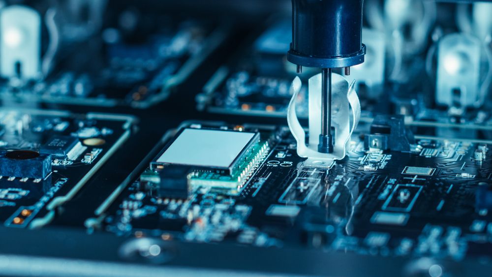
Because you cannot physically touch the middle of a 3D stack with a probe, the black box nature of advanced packaging requires robust Design for Test. Engineers must incorporate JTAG and internal self-test structures within the chiplet architecture itself to diagnose issues post-assembly.
Furthermore, software tools have become the backbone of successful integration. Platforms like Altium Develop provide power and signal integrity extensions that allow you to simulate the electrical and thermal profile of the entire package as a single, unified system. Simulating these complex interactions before manufacturing is the only way to avoid the nightmare of a costly re-design.
The Future Is Modular
The shift toward chiplets represents the most significant change in semiconductor philosophy in decades. By moving away from the monolithic everything-on-one-chip approach, we are opening the door for more flexible, cost-effective, and powerful electronics.
The future of electronics isn't just defined by what is etched on the silicon, but by how intelligently we can stitch it all together. For mid-market players, this modular revolution is the key to competing with the giants, providing a path to high-performance computing without the astronomical price tag of 2nm monolithic yields.
Frequently Asked Questions
What are chiplets, and why are they replacing monolithic SoCs?
Chiplets are small, functional dies that work together inside a single package. They replace large monolithic SoCs because smaller dies offer higher yield, lower cost, and better process‑node optimization. Instead of using expensive 3nm or 5nm silicon for everything, each chiplet can use the best node for its function, enabling more efficient and scalable designs.
What is the difference between 2.5D and 3D packaging?
2.5D packaging places chiplets side‑by‑side on an interposer or silicon bridge, enabling high‑bandwidth connections with short distances.
3D packaging stacks dies vertically using TSVs, putting memory and logic extremely close to each other for ultra‑low latency.
Engineers choose between them based on performance needs, thermal constraints, and system complexity.
Why is thermal management such a major challenge in 3D ICs?
Stacking dies creates a thermal sandwich, trapping heat in the middle layers. This can cause logic die hotspots, memory corruption, or premature device failure. To manage heat, engineers rely on:
- Thermal‑aware floorplanning
- Thermal TSVs (heat‑carrying vias)
- Micro‑fluidic cooling for extreme cases
These methods help maintain performance and reliability in dense, high‑power 3D stacks.
What is UCIe, and why is it important for chiplet ecosystems?
UCIe (Universal Chiplet Interconnect Express) is an open die‑to‑die interconnect standard that allows chiplets from different vendors to communicate. It solves the interoperability problem created by proprietary interfaces and reduces vendor lock‑in. UCIe is essential for enabling a true chiplet marketplace, where companies can mix and match components to build modular, high‑performance systems.

About Author
Related Resources
Related Technical Documentation
Table of Contents
- Key Takeaways
- Architecture: How We Stack the Deck
- 2.5D Packaging
- 3.0D Packaging
- The Thermal Sandwich Problem
- Solving the Tower of Babel Interconnect Problem
- Sourcing and Reliability: The Known-Good Die
- Partnering with the Golden Triangle
- Design for Test and Simulation
- The Future Is Modular
- Frequently Asked Questions
Design to Release, Without the Friction
- Keep reviews tied to the right version
- Reduce handoff confusion and rework
- Spot sourcing and release risk earlier
- Work solo, share when needed
Get Started
Thank you, you are now subscribed to updates.