


PCB Design Data Management Tips for Multi-Board Projects

At a Glance
Projects with multiple PCBs require multiple data packages to produce individual boards, and an assembly-level package with all the components incorporated.


A single piece of a project can generate a ton of data, so just imagine how much data is generated with a multi-board PCB project. Each PCB needs a standard set of PCB design outputs to manufacture an individual board, with each output being clearly named and marked. PCB manufacturers need the outputs from each individual board to produce and assemble them, as well as to prevent errors during the process.
PCB data management ensures we are keeping track not just of the data for individual PCBs, but also the assembly-level data. This assembly-level data will be used by a product assembler or your internal assembly team to build the final product, which can include mechanical elements like cabling and enclosures. I'll show you what all of it can look like in this article to help inform your processes and workflow.
Separate or Combined Data Packages?
Any products with multiple PCBs will have product or assembly-level data, as well as data for the individual PCBs in the assembly. How should your data packages for these elements be cataloged and linked together?
We have seen companies implement this in multiple ways. Without a good multi-board PCB design tool, many companies resort to a lot of copy and paste activity in order to make sure all of the PCB-level and assembly-level data lines up and is consistent. With a good multi-PCB design solution, it's easy to keep track of the individual boards within a single assembly, but the overall assembly still needs some additional information which must be input by the design team and the mechanical engineer.
We find that the optimal data hierarchy looks something like this:

Based on the above hierarchy, you can develop separate data packages for each of the main blocks, or you can create a product-level data package that includes all of the sub-assemblies within it. Which of these you develop depends on the capabilities of your PCB design tools and who needs to receive your data package. For example, PCB manufacturers only need the data packages for individual boards, while an internal assembly team only needs the assembly-level information.
Let's break into each one of these areas as shown in the hierarchy.
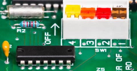
PCB-Level Production Data
Within a multi-board project, each PCB has its own standard PCB design outputs required to manufacture each board:
- Gerbers, ODB++, or IPC-2581
- Pick and place file
- Bill of materials with part numbers
- Drill files
- Fabrication and assembly drawings
Each PCB and PCBA should have a unique part number; the PCBA part number becomes important for denoting which design elements fit into the full product assembly. By breaking PCBs into individual projects like this, it will be easier to call them out in the overall assembly data.
A completed PCB data package for a multi-board project will eventually live in a PDM platform or, ideally, in a PLM platform. The PDM/PLM platform tracks all revisions and reviews of the product and acts as the single point of reference for the current revision of the project. There are two options for placing multi-PCB product data into a PDM/PLM: create separate PLM entries for each part of the product (Option 1), or create a single PLM entry for the entire product (Option 2).

We think that tracking each PCB within a single multi-board project (Option 2), similar to the above hierarchy, makes the most sense from a data management standpoint. Putting all the product data into a PLM entry with product-level reviews and approvals provides a single source of truth for all sub-assemblies in the product. Multi-board-capable ECAD software with a direct integration into major PLM systems expedites the implementation of Option 2.
Still, there are instances where Option 1 makes the most sense. For example, some companies create modular product lines which can be combined in various ways, or they re-use some designs in multiple products. In these cases, it does not make sense to duplicate PCB1/PCB2/etc. across multiple product instances in a PLM. Another instance that occurs at larger companies is when different business units use each other's designs in multi-board projects; Option 2 would also demand making copies of sub-assembly data across multiple PLM instances, creating multiple sources of truth and disrupting the standard PLM workflow.
PCB Libraries For Multi-Board Projects
Within each PCB is contained library parts, which may be part of distinct projects, and may even be maintained by different engineering groups or different companies. Library management for multi-board systems can be very complex due to the number of different stakeholders and participants who are creating the CAD data for all the PCBs and their components. How do you ensure parts data is accurate and CAD model standards are enforced across PCB projects?
Successful companies that build complex products often have a centralized library that is used for all projects, where a dedicated ECAD team can enforce standards and has control over any changes to symbols/footprints. These models then flow into the PCB data for each PCB in a multi-board assembly.

One challenge that arises relating to lack of consistency comes from working with external partner companies or contractors. External companies developing part of a multi-board system may have their own library standards and processes which make their way into the multi-board assembly data package. This is why it’s so important for a team’s PCB library to be accessible to external stakeholders through a cloud platform.
Product Assembly-Level Data
Most products that use multiple PCBs have additional components that do not appear in the BOMs of any of the individual PCBs. However, these additional components are required to build the overall product assembly and so they must be listed somewhere in the product-level data. This information needs to be stored somewhere and linked back to the individual PCBs in the multi-board system.
If you aren't defining a multi-board project for your product, you can create an assembly-level project in your CAD tool and specify each of the components in PCBAs as a line on the BOM. You can also define connections between PCBs in a schematic using the individual PCBA part number, reference designator, and applicable part number for any cabling. Part numbers for custom wire harnesses should also be included in these documents.

Notice how the product-level BOM specifies each of the PCBA part numbers that will be included in the product assembly. There are also part numbers for wiring harnesses, off-the-shelf cables, enclosure pieces, gaskets, and even crimp contacts for wire-to-board connectors. Each of these elements is reflected in most schematic diagrams showing the electrical connections in the multi-board assembly.
Multi-Board Assembly Drawings
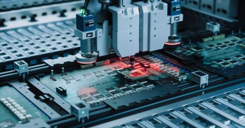
Multi-board designs will eventually need to be built into a physical product. To ensure this is done correctly, an assembly drawing is needed for the entire product, and individual assembly drawings are required for the PCBs in the multi-board system. The assembly drawing for each PCB should follow the typical format we expect, complete with assembly notes and a 3D view or assembly layer rendering directly in the drawing.
Assembly layer renderings for multi-board systems should show the arrangement of all the PCBs in the system, including the 3D models assigned to parts in each of the PCBs. The drawing is used as the basis for assembly of the entire system by a team after the individual PCBs are assembled and delivered for product-level assembly.

Another important role of a multi-board assembly drawing is to provide assembly instructions for the various boards. The drawing and its instructions are handed off to technicians who will put the stack of PCBs together and mount the PCBs into the product packaging.
- Instructions should state the order in which boards are assembled into their interconnected stack
- Any mechanical parts or fasteners should be detailed as part of the assembly instructions
- Enclosure or packaging (if included in the product) should also be listed in the product assembly drawing
- Handling instructions (ESD-safe handling, chemical exposure prevention, disposal, etc.) must be specified in the instructions
Assembly instructions should reference part numbers in the product-level BOM, including the PCBA part numbers so there is no confusion as to which parts are involved in each assembly step. Assembly instructions can also be created graphically in mechanical modeling programs; this requires transferring the electrical design into MCAD software in order to create realistic renderings showing graphical assembly steps.
Tracking and Releasing Multi-Board Assembly Data Packages
Once it’s time to produce a multi-board assembly, the individual data packages need to be pulled from the PLM repository and handed off to manufacturers. It’s common to put each PCB into different fabrication facilities due to the different capabilities and lead times required to produce each PCB in the product. This gives PCB buyers a way to control lead time and cost.
Data packages for multi-PCB products should be handled in much the same way as other designs: with a focus on data security and controlled release of information only to select parties. Procurement managers and engineering managers need to be able to control who receives specific parts of the multi-PCB data package.
Electrical Design:
- Separate data between fabrication and assembly
- Fabrication and assembly should not receive schematics
- Fabrication and assembly should not receive 3D models of the full assembly
- Do not send out product-level packages to each vendor; send only individual PCB data packages
Mechanical/Harness Design:
- Mechanical fabrication does not require any of the electrical data
- Procurement managers may need to separate mechanical elements from the product-level BOM
- Harness or cabling manufacturers do only require mating interface information, they don’t need to receive any electrical schematics
Once each portion of the multi-board design is produced, it can be sent into assembly to produce the final product. As the design is moved to the next revision, the entire package can be brought back into your design software to perform electrical and mechanical updates. Only Altium Develop unifies these disciplines through Altium Designer and mechanical integration in the MCAD CoDesigner utility.

To learn more about multi-board design and assembly, read about the physical assembly creation features in the Altium Documentation. These tools enable creation of 3D models for PCB assemblies which can then be handed off for enclosure design using the MCAD Collaboration features in Altium Develop. This allows mechanical engineers to see a draft assembly of your board array in industry-standard MCAD software like SolidWorks, and the product packaging can be designed around the 3D arrangement of PCBs.
Whether you need to build reliable power electronics or advanced digital systems, use Altium’s complete set of PCB design features and world-class CAD tools. Altium provides the world’s premier electronic product development platform, complete with the industry’s best PCB design tools and cross-disciplinary collaboration features for advanced design teams. Contact an expert at Altium today!
About Author
Related Resources
Related Technical Documentation
Table of Contents
Design to Release, Without the Friction
- Keep reviews tied to the right version
- Reduce handoff confusion and rework
- Spot sourcing and release risk earlier
- Work solo, share when needed
Get Started
Thank you, you are now subscribed to updates.

