


Common Printed Circuit Board Defects You Can Fix in the Cloud

At a Glance
Solve these printed circuit board defects you can fix with the cloud collaboration tools in Altium Designer.


Just like any other field of manufacturing, defects can occur in the manufacturing process, and some of these can be related directly to your design choices. Sometimes designs contain problems that can unintentionally cause defects, possibly due to incorrectly entering a design rule or forgetting to pay attention to an industry standard. Other defects might happen in fabrication or assembly that are not the fault of the designer.
New designs need to be put through a thorough design review by the manufacturer before fabrication, and modern cloud sharing tools are making this process much easier. When designs can be shared and reviewed in the cloud, you can speed up the review time and easily call out changes that might cause common printed circuit manufacturing defects.
Altium 365 is changing the dynamic around design reviews for remote PCB design teams by making everything available to manufacturers, customers, and other designers on a cloud platform. This is a great way to quickly move through a design review and callout design changes before fabrication in a single location. There are some common printed circuit board defects that can be spotted quickly thanks to Altium 365, either in the .PcbDoc file or Gerbers.
You Can Solve These Printed Circuit Board Defects in the Cloud
When projects are managed in the cloud, it’s easy to share designs and get feedback on anything that might reduce yield before you start fabrication. There are many design choices that can created manufacturing defects, and you can work with your team to correct these through Altium 365.
Tombstoning and Thermal Reliefs
Thermal reliefs are sometimes framed as an always/never argument, but they are useful for preventing tombstoning during wave soldering. Some designers demand they always be used in a design, while others say they’ve always assembled successfully without defects. No matter how you feel about thermal reliefs on plane layers, my feeling is the assembler should make the call on when they are included or removed. They’re the experts and they know their process, so take advantage of their experience.
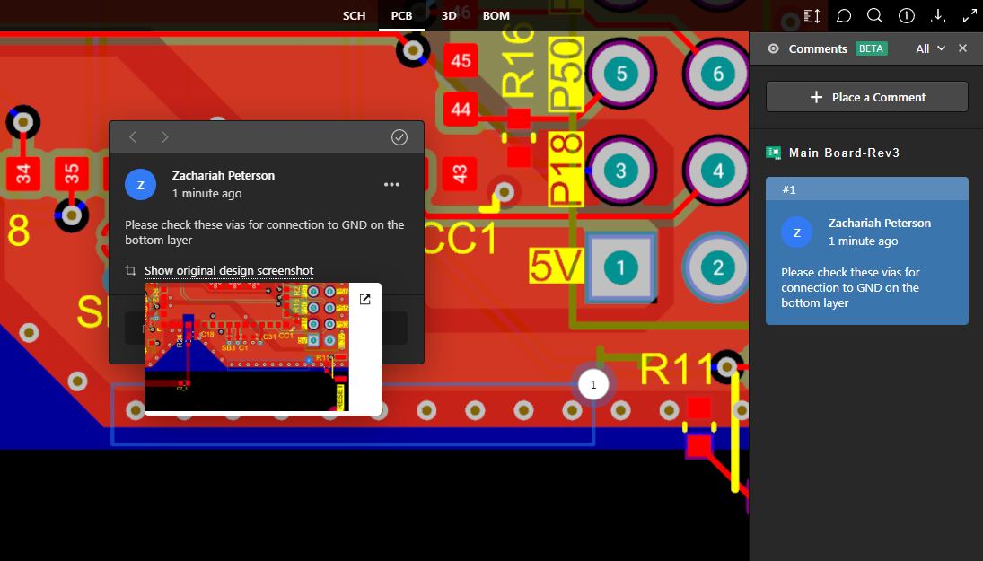
The presence (or absence) of thermal reliefs can be seen in the PCB layout directly in Altium Designer, or in the shared project view in the Altium 365 platform. The advantage of Altium 365 is that it allows sharing: a project can be shared with a fabricator or assembler, and the recipient can quickly open and scan through locations on plane layers where thermal reliefs are needed. They can also place comments on the design to call out vias that may need thermal relief on plane layers or large polygons.
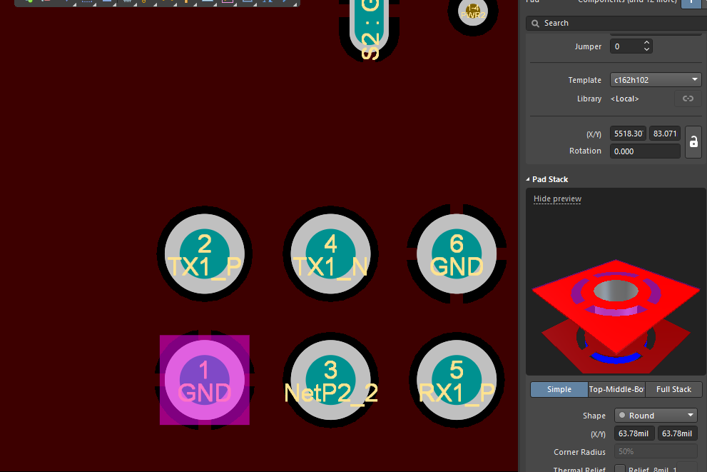
Disconnected Via and Plane/Polygon Connections
I got to experience this headache during a recent fabrication run. Thankfully, the fabricator got the board correct, but the boards were only fabricated correctly on accident. When you need to apply a feature like a shorted stub line for impedance matching, you’ll basically be creating a short circuit back to a grounded plane or polygon through a via. The clearance rules will take over and possibly limit the clearance between the polygon and via to the smallest possible value (1 mil in Altium Designer.). This is shown below for an example via fence.
During design, you need to either set the clearance to 0 mils, which then triggers a short circuit design rule violation. You can then just ignore the rule violation for that net. From the fabricator’s perspective, this undesired spacing can be on the back plane layer as long as the view is zoomed in close. A better way to spot this is to look at the Gerber files for that layer. Most fabricators should be able to spot this and flag it for review with the designer.
As a manufacturer, doing this through a managed project in Altium 365 lets you leave comments directly in the design documents, either through your web browser or through Altium Designer. The designer can then instantly view and correct the problem area in Altium Designer and save the changes back to the Altium 365 cloud platform. Once a comment is left on a project document, everyone watching the project will get a notification of the new comment and link to view the file in the Altium 365 web instance.
Clearances in General
Clearances are part of a larger set of possible printed circuit board defects, depending on whether you’re dealing with a high voltage board (to prevent ESD), high speed board (to prevent crosstalk), or SMT assembly (to prevent bridging during soldering). Altium 365 makes it easy to scan through the layout and spot potential clearance problems, flag these for a designer with comments, and notify the designer of these defects without sending a single email. The designer can then reopen the project in Altium Designer and make the required changes without emailing files back and forth.
Drill Hits
A mistake with a drill hit (either missing, overlapping, or extraneous) can be noticed when a Gerber file or NC drill file is compared to a fab drawing or dimensioned drill drawing in the PCB layout. This can happen when a design is updated, but the fabrication data simply isn’t updated. Manufacturers can comment on these problems with drill hits immediately in the PCB layout, and the designer will receive an email notifying them of the comment and required changes. This can be as simple as regenerating fabrication files or a significant design change to ensure drill hits are where everyone expects.
Manufacturers Often Inspect and Compare Gerbers
At the end of the day, your manufacturer is going to use your Gerber files to create your PCB stencil, not your PCB layout files. They might also use the IPC-2581 or ODB++ universal file formats. The manufacturers I work with prefer Gerbers as they are the de facto PCB fabrication file standard and everybody else understands them.
Everything I’ve shown above happens in the PCB layout files, but it can also happen in Gerber files. When an Altium Designer project is released to a manufacturer, the recipient can download and open the fabrication files in Altium Designer or another Gerber viewer program to do a design review. These utilities can run automated DFM checks and pinpoint printed circuit board defects. The manufacturer can then go back into the cloud instance and leave a comment with the required changes for the designer.
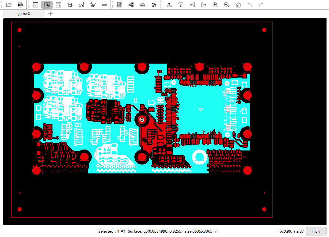
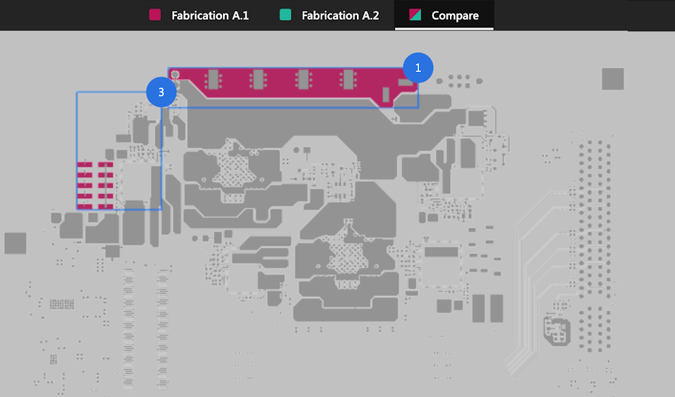
A manufacturer can also view and compare Gerber files through their web browser in the Altium 365 cloud platform. The new Gerber Compare feature in Altium 365 lets a manufacturer compare Gerber files from different Project Releases, so they can quickly spot when design defects have been solved and what has changed between each release.
Today’s PCB manufacturers and PCB designers can work together to eliminate common printed circuit board defects and get through production quickly thanks to the Altium 365™ platform. This unique cloud-based platform integrates with the world-class design tools in Altium Designer®, making all your project data accessible to your manufacturer and collaborators in a secure environment. Designers and manufacturers can share PCB fabrication data, project files, and much more in a cloud-based platform.
We have only scratched the surface of what is possible to do with Altium Designer on Altium 365. You can check the product page for a more in-depth feature description or one of the On-Demand Webinars.

About Author
Related Resources
Related Technical Documentation
Table of Contents
Design to Release, Without the Friction
- Keep reviews tied to the right version
- Reduce handoff confusion and rework
- Spot sourcing and release risk earlier
- Work solo, share when needed
Get Started
Thank you, you are now subscribed to updates.


