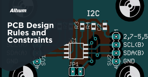


The Critical Role of Constraint-Based PCB Design in Modern Electronics


Welcome to the intricate realm of PCB (Printed Circuit Board) design, where what begins as a simple circuit board evolves into a sophisticated masterpiece of electronic engineering. As the backbone of modern electronics, PCBs breathe life into our everyday devices, from smartphones to laptops. Crafting a reliable and functional PCB extends beyond merely connecting components. It demands a meticulous understanding of various aspects to achieve optimal performance and manufacturability. Central to this endeavor is constraint-based PCB design—a strategic methodology that meticulously governs the physical and electrical characteristics of a PCB. Such constraints not only safeguard against manufacturing pitfalls but also ensure electrical prowess, culminating in a product that doesn't just meet the mark but sets new standards. In this post, we explore PCB constraints and how they play a crucial role in ensuring a successful design.
Grasping Constraint-Based PCB Design
Constraint-based design involves defining parameters that dictate how a PCB should be constructed. These constraints encompass multiple aspects, including electrical, physical, and manufacturing considerations. Considering constraints early in the design process is crucial, as it sets the groundwork for a successful design that aligns with the project requirements and end goals.
Constraint-based PCB design is akin to a maestro orchestrating a symphony. It balances numerous requirements to shape the overall design process, ensuring a harmonious outcome. These constraints can vary:

-
Electrical Constraints:
-
Trace Width and Spacing: Defines the width and spacing of traces to ensure proper current carrying capacity and avoid short-circuits.
-
Via Sizes and Types: Specifies dimensions and types of vias, based on design requirements and manufacturing capabilities.
-
Impedance Control: Ensures traces are designed to have specific impedance values, crucial for high-speed designs.
-
Clearance: Defines the minimum distance between different electrical entities (like traces, pads, vias) to avoid short circuits.
-
High-speed Constraints: Rules related to the design of high-speed circuits, including length matching, differential pair routing, and phase control.
-
-
Physical Constraints:
-
Board Dimensions: Specifies the size and shape of the PCB.
-
Layer Stackup: Defines the number and arrangement of copper and insulating layers in the PCB.
-
Component Placement: Provides guidelines for placing components on the board, ensuring they don't interfere with each other and adhere to thermal and mechanical considerations.
-
Thermal Constraints: Ensures areas generating high heat have sufficient thermal relief, including the use of heat sinks or thermal vias.
-
-
Manufacturability Constraints (Design for Manufacturability - DFM):
-
Solder Mask Clearance: Ensures that solder masks are appropriately applied to avoid short circuits during the soldering process.
-
Silkscreen Overlap: Ensures that component labels or other silkscreen elements do not overlap with pads or vias.
-
Hole Sizes: Specifies the minimum and maximum sizes for drilled holes based on manufacturing capabilities.
-
Annular Ring Size: Defines the minimum width of the copper ring around a drilled hole.
-
Copper-to-Edge Clearance: Defines the minimum distance required between the edge of the PCB and any copper feature.
-
-
Assembly Constraints (Design for Assembly - DFA):
-
Component Orientation: Ensures components are correctly oriented for automated assembly.
-
Component-to-Component Clearance: Ensures sufficient space between components to allow for assembly and avoid interference.
-
Polarity and Pin 1 Indicators: Guidelines for marking components to ensure they are placed correctly during assembly.
-
-
Reliability Constraints:
-
Flex and Bend: Defines regions that can and cannot be bent in flex PCBs.
-
Vibration and Shock: Constraints to ensure components can withstand specific vibration and shock levels, especially in rugged applications.
-
-
Testing Constraints (Design for Test - DFT):
-
Test Point Requirements: Specifies the number and placement of test points for in-circuit testing.
-
Access for Probing: Ensures test equipment can access critical nodes during testing.
-
-
Environmental and Regulatory Constraints:
-
RoHS/Lead-Free Design: Ensures PCBs are designed to adhere to environmental regulations, like the Restriction of Hazardous Substances (RoHS).
-
Electromagnetic Compatibility (EMC): Ensures designs adhere to electromagnetic interference (EMI) and susceptibility requirements.
-
Advantages of Constraint-Based PCB Design
- Enhanced Signal Integrity and Reliability

In the world of electronics, signal integrity is paramount. Constraint-based design minimizes electromagnetic interference (EMI) and ensures proper trace routing for impedance control. By optimizing ground and power planes, noise is reduced, leading to improved signal reliability.
- Improved Thermal Management

Efficient heat dissipation is a challenge in compact electronics. Constraint-based design tackles this by strategically placing components, utilizing thermal relief, and integrating sensors for real-time temperature monitoring. This ensures that devices maintain optimal operating temperatures.
- Streamlined Manufacturing and Assembly

Designing for manufacturability (DFM) is a key concept. Constraint-based design includes component placement rules that facilitate automated assembly, reducing errors. By considering various soldering and assembly techniques, manufacturing becomes more seamless.
- Faster Time-to-Market

Time is of the essence in the competitive electronics market. Constraint-based design reduces the need for countless design iterations by identifying flaws early through simulations. Collaborative design involving cross-functional teams also expedites the process.
- Cost Savings

Design re-spins are expensive and time-consuming. Constraint-based design minimizes these by ensuring the initial design aligns with requirements. Efficient layouts optimize material usage and eliminate the need for costly post-production modifications.
- Compliance and Standards

Electronic products must adhere to regulatory standards. Constraint-based design aids in designing with EMC, safety, and other industry standards in mind. This simplifies the certification process and ensures products meet legal requirements.
Implementing the Methodology
Design Rule Check (DRC) is a fundamental step in the PCB design process. It involves checking the design against a set of predefined rules to ensure the PCB will be functional, manufacturable, and reliable. Implementing DRC in your PCB design process helps catch errors before manufacturing, reducing costly re-spins, and potential functional issues.
Here's a step-by-step guide on how to implement DRC in PCB design:
-
Understand Manufacturing Capabilities:
-
Begin by gathering the capabilities and constraints from your PCB manufacturer. This might include rules related to trace width and spacing, via sizes, hole sizes, annular ring sizes, and whatever you need to set your design up for success.
-
-
Set Up the Design Rules in Your PCB Design Software:
-
Most modern PCB design tools include a design rules setup or configuration section;
-
Enter the manufacturer's constraints and any additional rules you need for your specific design. This might include electrical rules, high-speed rules, thermal rules, etc.
-
-
Layer-specific Rules:
-
Some rules are specific to certain layers. For example, the top and bottom layers might have different trace width and spacing rules compared to inner layers. Make sure to define these layer-specific rules.
-
-
Run the DRC:
-
Once your rules are set up, you can run the DRC. This will usually generate a list of violations or errors based on the rules you've set;
-
Some common violations might include trace width violations, clearance violations, unconnected nets, and overlapping components.
-
-
Review and Address Violations:
-
For each violation, the PCB design software typically provides a description and a visual indication of where the issue is on the board;
-
Go through each violation and correct the issue in the design. This might involve moving components, rerouting traces, or adjusting the design rules if they were set up incorrectly.
-
-
Iterative Process:
-
After correcting known violations, run the DRC again to ensure that no new issues have been introduced and all previous ones have been resolved;
-
This might need to be repeated several times until no violations are found.
-
-
Additional Checks:
-
Beyond standard DRC, consider running other checks like Electrical Rule Check (ERC) to catch logical and connectivity errors, or a Differential Pair Routing Check for high-speed designs.
-
-
Document Any Deliberate Violations:
-
In some cases, you might choose to violate a rule deliberately for a specific design requirement. In such cases, it's essential to document this decision, explaining the rationale and ensuring the manufacturer is aware of it.
-
-
Collaborate with the Manufacturer:
-
Before finalizing the design, it can be beneficial to send the design files to the manufacturer for review. They might run their own DRC and provide feedback based on their specific manufacturing processes.
-
-
Stay Updated:
-
Manufacturing capabilities and standards can change over time. Periodically review and update your design rules to ensure they align with the latest capabilities and industry best practices.
-
Wrapping Up
The world of electronics is in perpetual flux, with innovations emerging at breakneck speeds. Amidst this, constraint-based PCB design emerges as a beacon, illuminating the path for designers. By meticulously defining, applying, and validating constraints, designers can craft PCBs that aren't just functional but also efficient, cost-effective, and superior in quality. In an age where precision and speed are paramount, can you afford to design any other way?
Whether you need to build reliable power electronics or advanced digital systems, Altium Develop unites every discipline into one collaborative force. Free from silos. Free from limits. It’s where engineers, designers, and innovators work together as one to create without constraints. Experience Altium Develop today!
About Author
Related Resources
Related Technical Documentation
Table of Contents
Design to Release, Without the Friction
- Keep reviews tied to the right version
- Reduce handoff confusion and rework
- Spot sourcing and release risk earlier
- Work solo, share when needed
Get Started
Thank you, you are now subscribed to updates.

