Customize designs with Consistent and Flexible Custom Rules and Queries
In the early stages of a circuit design, I frequently consider mechanical dimensions along with circuit requirements. Knowing dimensions of large components helps me visualize where they will fit with respect to overall three-dimensional device enclosure and the board’s location within the space. During the thought experiment for fit, I begin making notes about tolerances I’ll push as a tradeoff between electrical functionality and mechanical dimension.
These close tolerances will need to be managed closely throughout the design cycle. Schematic capture and PCB layout tools are blank slates and their environments have selectable options for setting up to design. For each project, the blank slate is made into a structural frame where some ideas take flight and others fail to get off the ground.
Having applicable tools to enable creative solutions in numerous ways helps designers innovate. When tools fail to provide solutions, ideas are lost and companies suffer.
Unacknowledged Custom Rules Cause Multiple Design Rule Check Errors
I’m grateful when I get into my schematic capture and PCB layout tools and the commands I intuit are found in the pulldowns. After defining the environment in exquisite detail, imagine my disappointment when those custom rules fail to follow the circuits designed into the layout. Although I set up the environment in my schematic editor, it failed to export the rules to layout and all was lost. More, I didn’t find this out until after I placed and routed the board.
It was found during a design rule check (DRC). The DRC produced a profusion of errors. The sheer amount of errors caused concern and it took me a moment to realize the DRC didn’t recognize the custom rules I set up for close tolerances. Settling in to perform a query took me off the task at hand. Trying to query for the custom rules required sinking time to learn the cryptic programming algorithm for actually writing a query.
It became apparent that understanding how to query in this layout software would take time and experience within the tool environment. And time to learn a command function wasn’t helping the project move along.
Finding and fixing PCB errors with custom rules
Design Rule Check Errors Result From Programs That Do Not Communication
Spending time on a steep learning curve for side work within a layout program is not ideal. Finding out that the tool I was using did not port commands left me concerned for two reasons. One was that I didn’t find out until after I’d laid out the board. I’d spent time during schematic capture to set up the exquisite environment necessary to push the tolerances.
Once I got to PCB layout, the custom commands I originally set up were gone. The other was the worry that I’d miss a real error hiding amongst all the pseudo-errors generated. I’d have to sift through all the conflict flags, which were many, and this may cause me to miss a true custom rule violation. Missing a real error could result in manufactured boards that may not work once they arrived at our factory.
I was losing confidence in the tool, given the lack of unified features. How could I reliably trust the developers to deliver a tool that was built to complement the original design captured in the schematic? I tried to run a query, hoping to select the known nodes from my custom rule. This was problematic as the query required learning the programming syntax for searching rather than using simple keywords within the search bar. It was going to be a long week.
Setting custom tolerance rules help organize close components
Apply Queries With Unified Tools Across the Design Environment
I was beginning to wish I had an environment where custom rules set up in the schematic would port, seamlessly, to the layout software when the time came for handoff. I imagined a well-organized process for defining the board constraints and rules would allow a well-defined environment.
If the constraints and rules could be organized outline style with levels to address each situation within the design would be ideal. Having intuitive commands in the pulldowns with the ability to follow the design through the entire process from schematic capture to PCB layout and then output file generation would be great.
It would be great if those commands extended to queries easily set up and tailored for the feature I was searching. Easy setup of searches depends on searchable keywords with filters to refine the search query. Know I could search in non-programmable language with direct translation for the query command goes a long way towards building intuition with the tool.
The query would search not only common rules but would search custom rules. Eliminating error messages for custom rules means I can see true errors when running a check. Dealing with real errors after the DRC would make me confident when I released the drawings to manufacture the board.
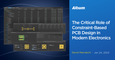
Altium Designer 18 has a PCB Editor and uses the concept of design rules. The editor has an intuitive hierarchy representing blocks of the layout, so nothing is missed. Specific areas included target electrical, routing, SMT, mask, plane, testpoint, manufacturing, high speed, and signal integrity. Should you have a need to add a custom rule in any of those categories, it is easily included within the editor environment.
In addition, Altium Designer 18 has both a Query Helper and a Query Builder. Both query tools are keyword driven, intuitive with a shallow learning curve. Applying the tools becomes as easy as pulling down a menu to activate a command.
If you’d like to know more about either the design rules or the query capability, talk to an expert at Altium today.


