Easing PCB Navigation with Snap Options

Accurate navigation in PCB design software is one of the many pain points that PCB designers face during initial component placement and throughout the entire design process. Snap options not only ensure accuracy, but speed placement, helping the process to run smoothly and ease the designers’ frustration.
INTRODUCTION
In PCB design, there are many actions such as placement, routing, alignment and length tuning that require heavy use of the mouse cursor. As you navigate during design, additional clicks required or incorrect objects selected can add to frustrations throughout the process. Snap options ensure accuracy, but speed placement can help the process run smoothly and ease your frustration, especially when deadlines are looming. This paper describes some tricks when using Altium that can save you time and make your PCB navigation with snap option design and navigation experience more rewarding.
ENHANCED SNAP OPTIONS IN ALTIUM
Having the ability to snap to many different available objects and/or primitives can be very useful in the PCB design process. Altium provides the capacity to snap to grids, guides and objects, including snap options to all layers, board outline and arc centers. The user-controlled grid1 can be used to make placement easier by allowing you the ability to snap to a defined grid, while work guides and point guidesare also controlled by the user and facilitate placement if used as a snap point. Image 1 below shows a few examples of these basic snap options.
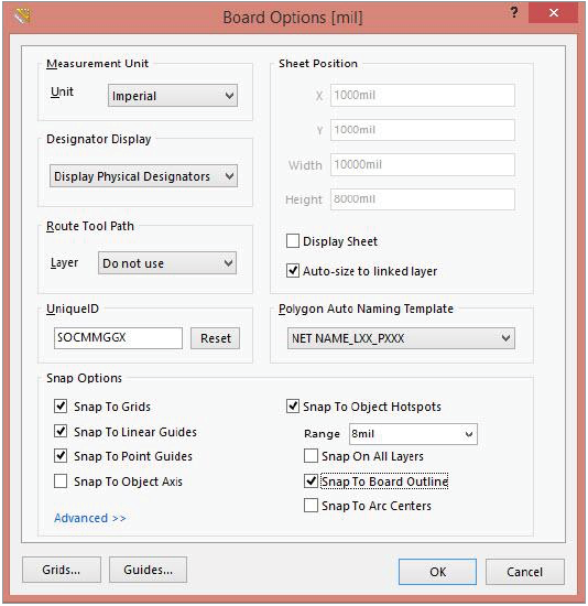
Image 1: Snap options
In Image 2 below, a vertical snap guide and a point guide were conveniently placed in the desired location. Even if the grid is changed, these guides will remain in their original location and can still be used as snap points. These guides are used as a snap point for the vias, even though they are off-grid.

Image 2: Object snap points
The ability to snap to the board outline improves the board dimensioning process. This specific snap feature to the board can also facilitate other applications such as castellated vias and mouse bites since a particular pad or via can snap directly on a board edge. Delving into the snap options a little further, the use of objects axes as snap points allow you to explore the many benefits of advanced snap options.
ADVANCED SNAP OPTIONS
More advanced techniques will require more advanced options that can ease the execution of such methods. Within Altium Designer, a set of advanced snap options can be configured, which will allow the cursor to align or snap to a particular object axis once within a specified range. Pads, vias, tracks, arcs, fills, regions, and text are all available objects that can be enabled for these tasks. Image 3 shows how you can enable these snap options.

Image 3: Advanced snap options
CONCLUSION
We know there are many factors we can’t control during the PCB layout design phase of a project; however, we can control the features used to enhance and guide PCB navigation with snap option design. Specific requirements for placement are inevitable, but optimizing on advanced snap options can significantly minimize the pain involved in the design environment. Getting the most out of the snap options in Printed Circuit Board design software will ultimately guide you through the entire Printed Circuit Board design process, saving you time and alleviating frustration.

