Group Components into Rooms for More Efficient Layout

The key to properly managing your component placements and traces is to utilize different techniques of grouping objects together rather than individually modifying each individual object. A lot of users hate the idea of having to individually bring a component to the board layout. This paper details what Altium Designer can do to make layout management easier and less time consuming, allowing you to meet your project deadlines.
INTRODUCTION TO GROUPING PCB COMPONENTS
A PCB group components layout can become really messy if the components and traces are not organized properly. The most common method of a managed design layout is through the use of rooms. Rooms can be used to manage design component placement better, and it can easily help one identify the component’s origin, which is explained more in detail below.
A rat’s nest of connections can be a pain as well because if no routing was performed and a lot of components are used. It will consume additional resources to produce connection lines across the layout, significantly decreasing system performance and making component placement much more difficult. The tangle can be enough to want to hire out for PCB design services, but there is a better option to keep your PCB designers in-house.
USING ROOMS IN ALTIUM DESIGNER
Rooms are commonly used to expedite the data transfer from the schematic to the PCB components layout editor, where each is defined as respective schematic sheet designs. This makes for a better Printed Circuit Board design and data management throughout the PCB fabrication process. The electronic components are defined on each sheet as component classes, in which its generations are defined through the project’s configurations. For example, a project contains 5 different sheets, each containing a specific PCB group components layout, in which the importance of a flat versus hierarchical design is voided. When the schematic is pushed over to the PCB layout of the project, the Printed Circuit Board design and layout will contain the sheet-defined rooms data with the respective electronic components used, illustrated in Figure 1. For components that are not already placed within a room after ECO generation, you can manually define a room over them or drag the component parts to the new room for future design updates.

Figure 1: Generating a room with the sheet-linked components.
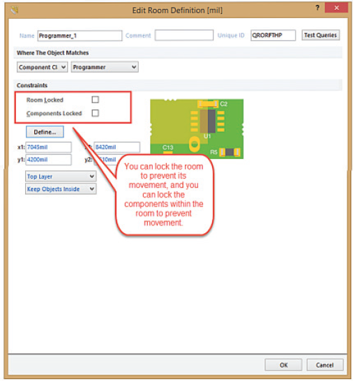
The neat thing about rooms is the room preference settings which allow for room data and component parts locking. With Printed Circuit Board components locked within a room, shown in Figure 2, you can relocate the room and bring all the assigned components along with it in one mouse-drag action, and then keep the room stationary using room locking. This removes a user’s hassle of manually moving each individual object or data, or a selection to group PCB components and objects for a preferred circuit board layout. Of course, the added capability to unlock the electronic components to individually relocate each one is an option too, allowing for optimal versatility in case modifications to one object or design may be required.

Figure 2: Rooms can be locked to prevent moving.
HIDING NETS
User-defined nets are assigned to specific objects within the Printed Circuit Board layout, defining the connections to be made. For example, BGAs have multiple vias and pads encompassing various nets waiting to be connected to other objects within the layout. When the BGA is left unrouted, a rat’s nest of connections will appear, which causes a visual confusion on component spacing and disrupts component placements. This can be easily resolved by hiding them, which can be performed for specific nets, Circuit Board components, or both.

Figure 3: Hiding the unrouted package allows you to see what you are routing without the rat’s nest of nets.
CONCLUSION
In summary, the utilization of rooms and appearances within a board layout can simplify your layout of components. If the Printed Circuit Board design tool didn’t contain such features, you would spend a large amount of time laying out a PCB board, and possibly result in not meet the deadlines. Who would have thought that colors and grouping can make a large difference to a component placement layout?


