


Getting Started with the GreenPAK Introduction Kit

At a Glance
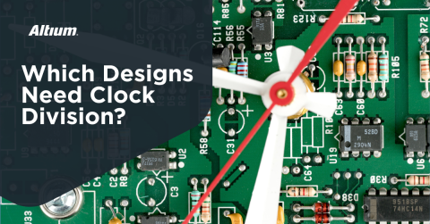
Explore Renesas GreenPAK. Build your first clock divider with schematic design, simulation, and oscilloscope testing using the intro kit.


As an engineer wearing many hats, I recently put on my firmware cap and tested out the Renesas GreenPAK Programmable Mixed Signal Kit and was rather intrigued. While I’ve dabbled a bit in mixed signal design, I tend to over-engineer solutions with microcontrollers and FPGAs in preference to designing a brand new circuit. Simple clock dividers become complex software. Power sequencing becomes power “state machines” with eventual software overhead that seems unnecessary. Conversely, I also may not have the time (or even know how) to implement all the circuitry on a board, especially if it requires a new board spin. This seemed like the perfect alternative that both firmware and hardware engineers could take advantage of. In this article, we’re going to look at getting started with the Renesas GreenPAK Programmable Mixed Signal Kit and demonstrate how to put together a simple clock divider circuit end-to-end.
What We’re Building
In order to demonstrate how to use the boards and the companion tool, we’re going to put together a very simple clock divider circuit. While this is a trivial example, it demonstrates, end-to-end, how to configure the device and use the Renesas Go Configure Software Hub. In this software, we’ll be able to control the hardware and also simulate our circuit as well. This will give us confidence that our circuit diagram is correct before running anything in hardware.
The Gear and Software
To get started, you’ll need the GreenPAK Advanced Development Board, the SLG4SA-DIP Adapter, and at least one DIP board (the SLG46721V-DIP specifically for this tutorial). The GreenPAK Introduction Kit comes with everything in one package so your best bet is just to pick up that kit. To fully validate everything is working, you’ll need to hook the output pins to an oscilloscope. I like using the Analog Discovery from Digilent (which is what will be used in this tutorial). It’s compact, lightweight, and not terribly expensive. It can be controlled with Python scripts which makes it super convenient for automation. You will also need to download and install Renesas Go Configure Software Hub.
Setting Up Your First Project
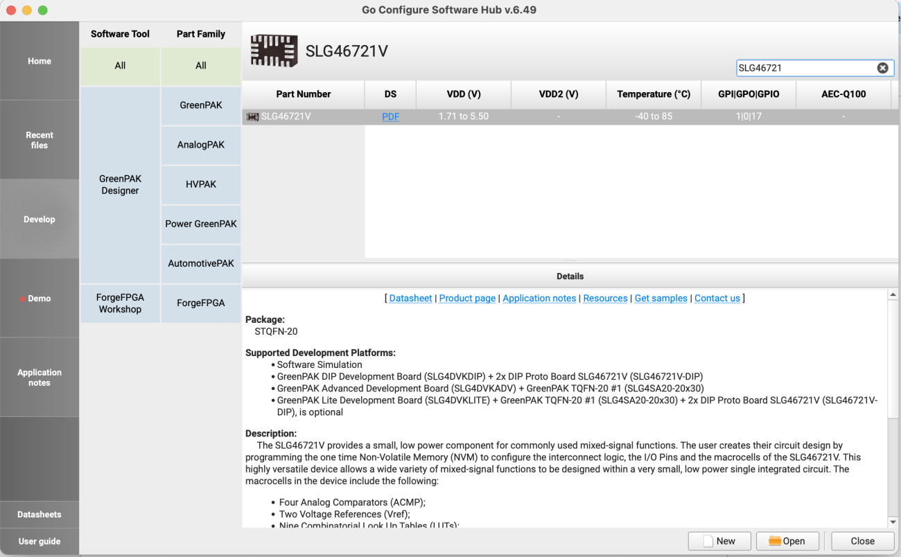
To get started, open up the Go Configure Software Hub and click on the “Develop” button on the left-hand side. In the search bar (on the top right-hand corner), enter “SLG46721” and you’ll see our target DIP show up. Make sure it’s selected and click the “New” button at the bottom of the window:
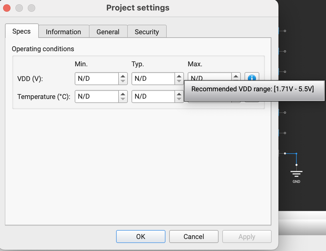
You’ll see a new window pop up called “Project Settings.” All of the defaults can be left alone except for VDD and temperature. If you click on the info icon on the right, it will tell you what the range should be. I set the typical voltage to 3.3 and set the typical temperature to 25.
After clicking OK, you will be greeted with an (almost) empty canvas:
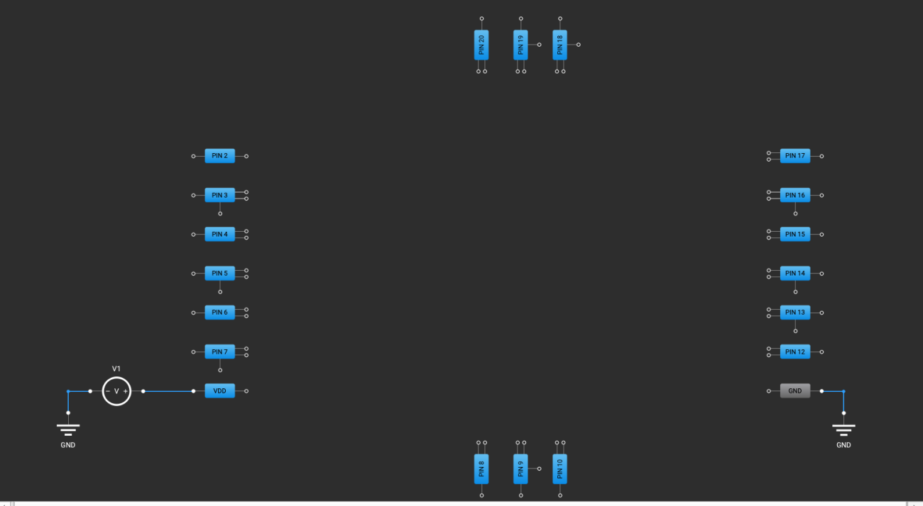
On the right-hand side of the Go Configure Software, you will see a bunch of checkboxes under “Components.” We want to check the following items:
- VDD (Pin 1)
- Pin 5
- Pin 6
- GND (Pin 11)
- OSC
- POR
You should leave the remaining checkboxes unchecked. At this point, you’ll have a few components that are sitting in your schematic. We’ll need to connect the components like so:
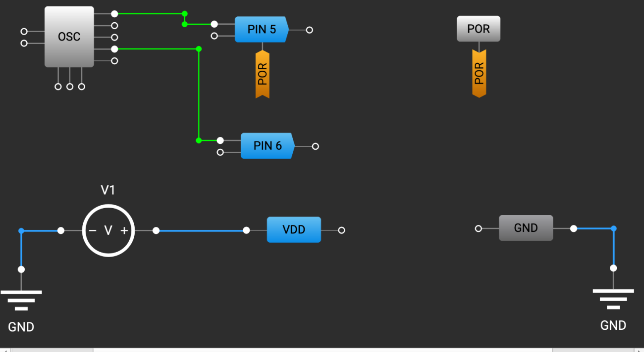
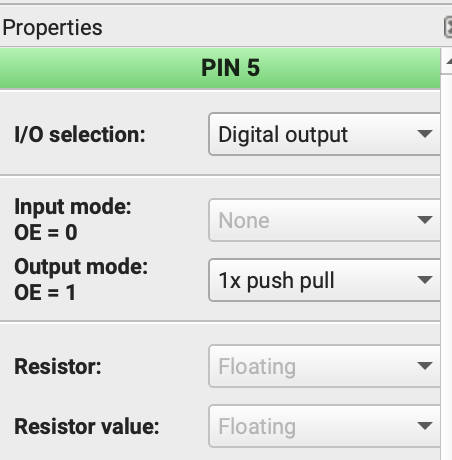
We need to modify the properties of some of these components as well. Let’s start by double-clicking on Pin 5 and navigating to the box on the left-hand side. Change the “I/O selection” dropdown to “Digital output.”
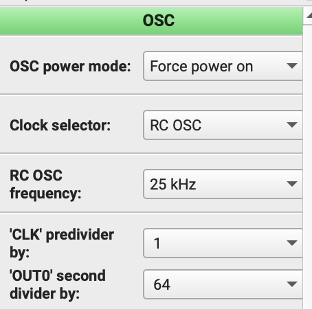
Do the same for Pin 6 as well. After that, right click on Pin 5 and click on “Flip horizontally.” This will line up the input port nicely against our oscillator. Do the same for Pin 6 as well. We’re almost done but we need to change one more setting for the oscillator component as well. Double-click on the OSC component and navigate to the properties window, just like we did with the pin ports. We will need to change a few parameters including “OSC power mode” and the “‘OUT0’second divider by” like so:
Assuming you’ve connected everything per Figure 4, we’re now ready to move onto simulation.
Simulating the Design
Now that our schematic is complete, we are ready to start simulating the circuit. Clicking the “Debug” button at the top of the toolbar opens a side panel on the right:
Click on the “Change platform” button and select “Software simulation.”
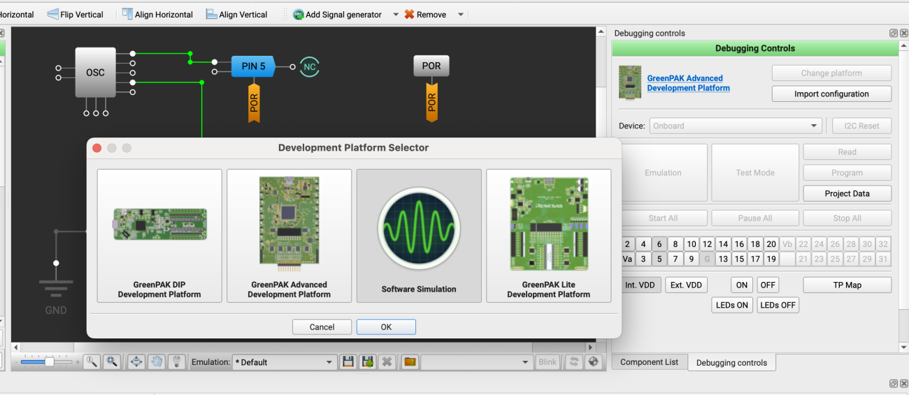
We first need to add “Test probes” to our schematic so we can monitor the signals (just like we do in most modern SPICE tools). Right underneath the debug button, you’ll see a button called “Add probe.” Click on that and then click on the inputs to Pin 5 and Pin 6. This will enable us to monitor the signals that will be going into those pins (i.e. what we will see on our oscilloscope). We can accept the defaults and just click on the “Start simulation button” on the right panel. This will bring up a new simulation window (after loading).
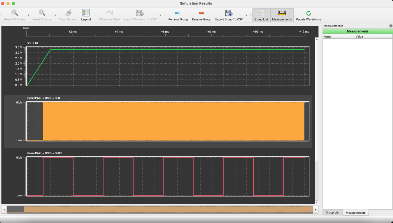
We can zoom in by left-clicking on the waveform and dragging our cursor across it. You can calculate the frequency and confirm that the top clock is 25 KHz and the second signal below is 25KHz/64. Now that we’re confident that our schematic is correct, we can run this on our hardware.
Running the Design in Hardware
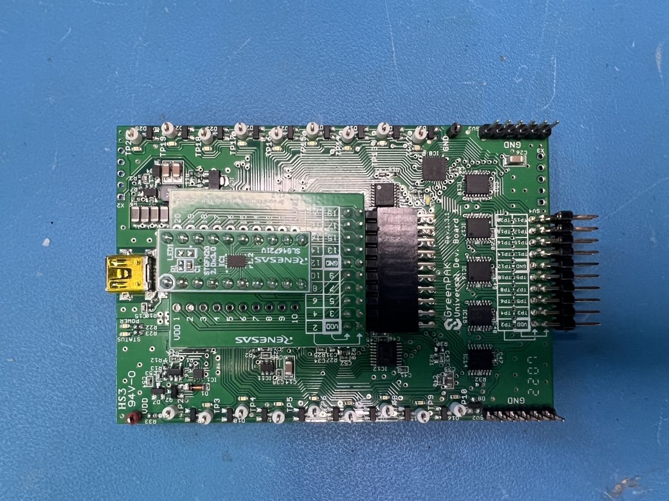
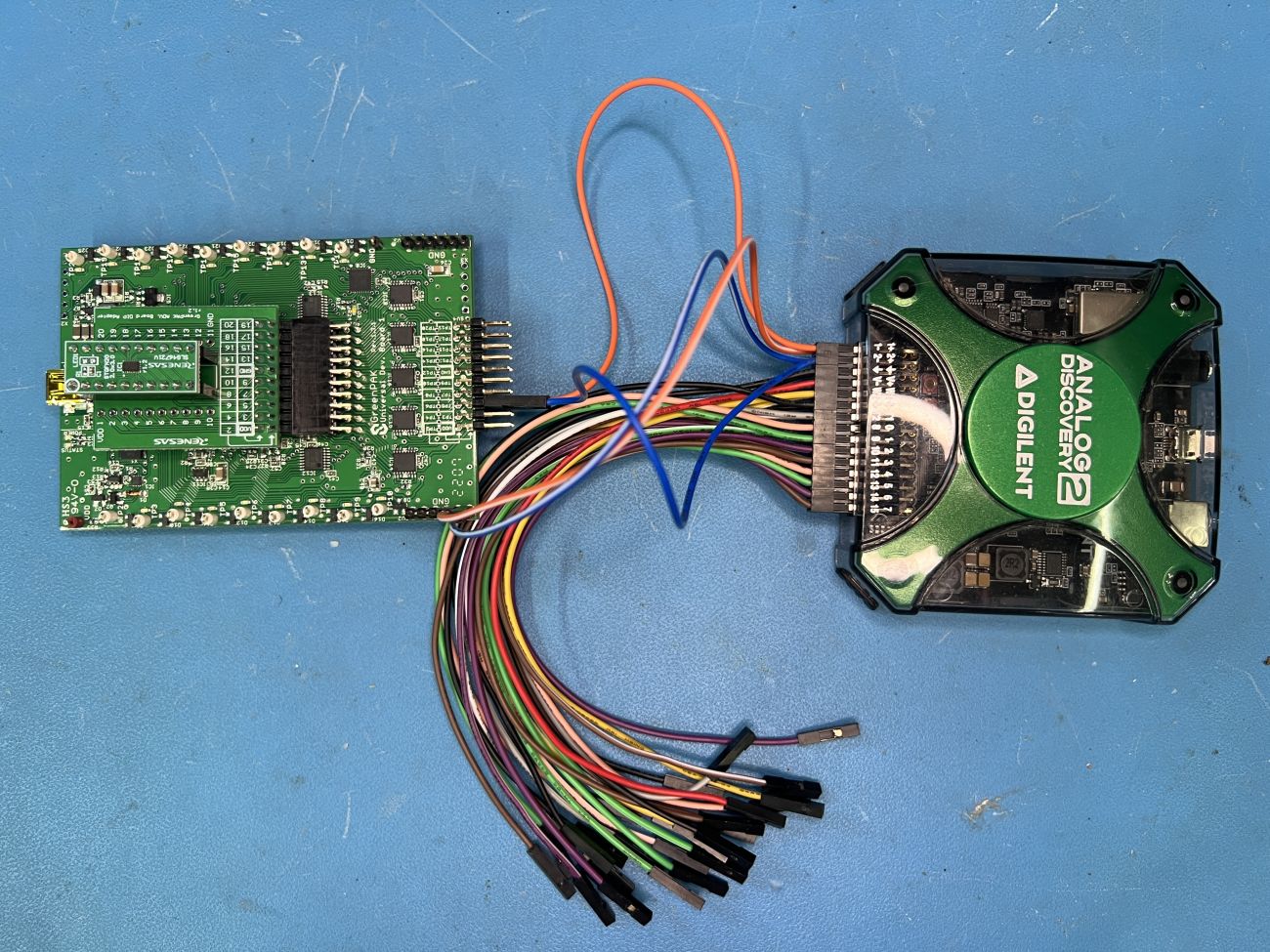
Just like the simulation option under “Change platform” we will want to change our platform to the “GreenPAK Advanced Development Platform” to match the evaluation kit that we have. Make sure your device is assembled and connected via USB. This means that the SLG46721V-DIP board is assembled onto the SLG4SA-DIP Adapter and that adapter is plugged into the GreenPAK Advanced Development Board.
You’ll be greeted with a panel that looks like this:
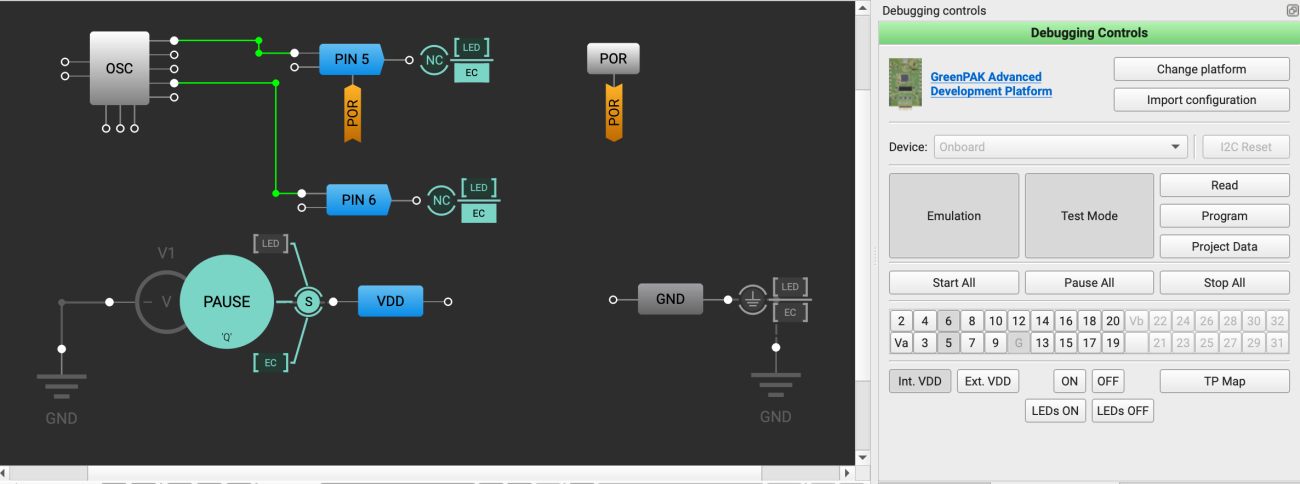
Click on the “Emulation” button on the right first to turn on the device. Then hover over the outputs of the PIN 5 and 6 ports and click on “EC” (which stands for external connector). This will direct the outputs to the output pins on the evaluation motherboard, which makes it super easy to plug in jumper cables into it like so:
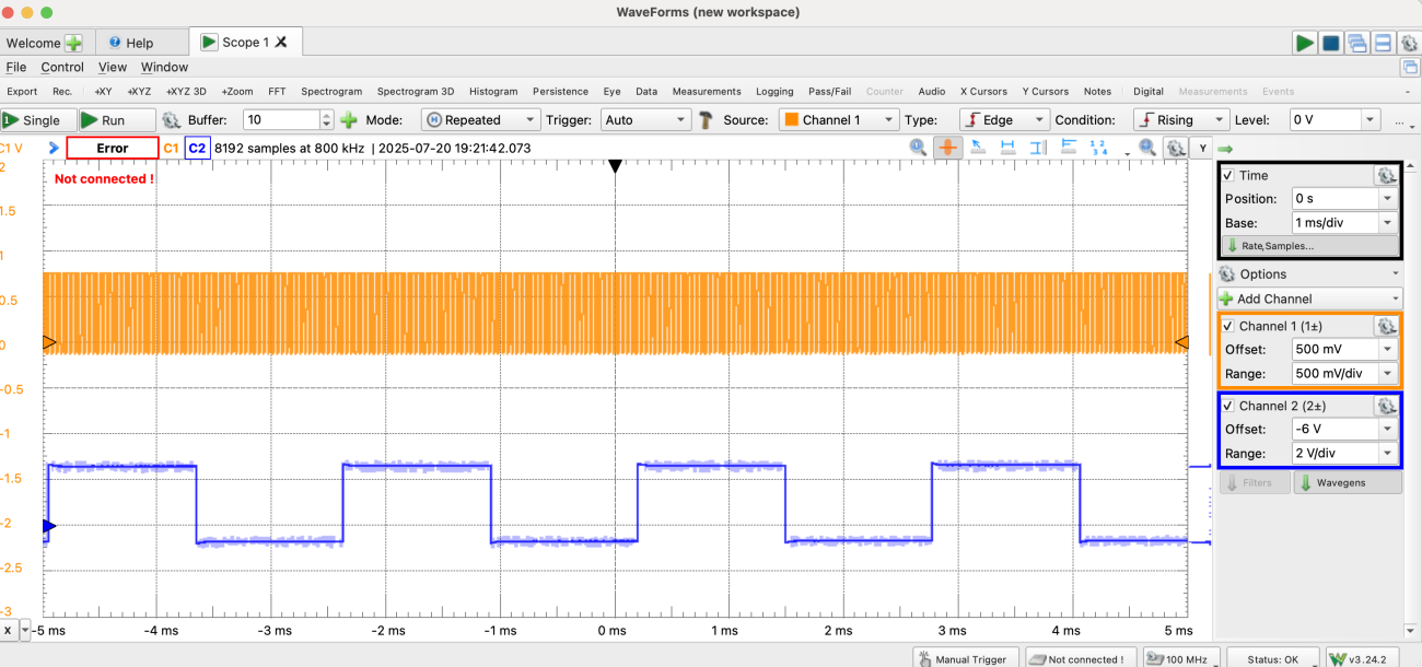
And now you can observe the signals directly on your oscilloscope. In this case, I’m using my Analog Discovery 2 with the Waveforms software in Oscilloscope mode:
Conclusion
We’ve now completed the tutorial to bring up the GreenPAK evaluation kit including schematic design, simulation, and hardware testing. You should now be able to start experimenting with more complex mixed signal designs using this DIP or other ones that are provided in the GreenPAK Introduction Kit.
About Author
Related Resources
Related Technical Documentation
Table of Contents
Design to Release, Without the Friction
- Keep reviews tied to the right version
- Reduce handoff confusion and rework
- Spot sourcing and release risk earlier
- Work solo, share when needed
Get Started
Thank you, you are now subscribed to updates.