
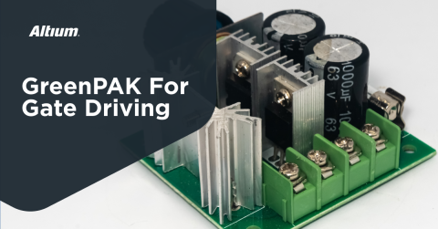


How to Keep Custom Logic in Small Board Space

At a Glance
Custom logic with mixed signal processing requires a large number of components and complex programming, such as with a CPLD or FPGA.


Processors allowing implementation of custom logic have traditionally been physically very large and difficult to develop. This has normally been appropriate because they are used for chip prototyping or to build application processors for embedded systems requiring high I/O count and compute resources.
To help engineers balance between system size, cost, and development effort, this article gives a comparison of the options for building digital and mixed signal systems with custom logic. Concentrate on when custom logic is needed, as it often causes designers to start hunting for smaller, more efficient processor options. This is definitely the case when the signal sensing is integrated with custom logic, as this can require a dozen or more components just to create the system analog front end.
Custom Logic Components Comparison
Custom logic can be programmed in silicon with three types of digital components:
- Field Programmable Gate Array (FPGA)
- Complex Programmable Logic Device (CPLD)
- Specialized processors like mixed signal processors
Each of these options provides the ability to develop custom logic but carries trade-offs between capability, cost, power, development effort, and board space.
FPGAs
Traditionally, FPGAs were used for system-level or chip-level prototyping, but they can also be used as the main system processor when off-the-shelf options do not meet technical requirements. Vendor IP for FPGAs enables instantiation of a processor core that can run an embedded OS as well as implementation of custom logic for specific computing tasks. With certainty, these components are the highest compute options for processors that allow for development of custom logic.

Of the three component types that enable custom logic, these components are physically the largest, carry the highest price tag, and require the most effort and experience to develop. Vendor IDEs and IP are helpful for building a chip design with the necessary interfaces and features, but custom logic instructions have to be coded.
Another downside of FPGAs is power consumption. FPGAs are known for consuming a lot of power, especially if the embedded design is not highly optimized. Many FPGAs require a large number of power regulators to support all of the required pin banks and rails. This additional component cost, design effort, and board space requirements makes almost all FPGAs unsuitable for small embedded systems that require very targeted, highly specified custom logic operations.
CPLDs
CPLDs provide a compact option for custom logic when board space is limited. These devices integrate a moderate amount of logic resources and I/O pins into a standard package, typically in a QFP. They consolidate discrete logic, decoders, and state machines into a single component.
Compared to FPGAs, CPLDs have a simpler architecture and consume less board area and power, making them a good fit for control applications, glue logic, or interface bridging. Designers can often fit a CPLD alongside a microcontroller or mixed-signal IC to add configurable digital functionality to an embedded system. A typical system block diagram would like that below, which shows the amount of space that would be required from even a small CPLD.

CPLDs offer a balance of development ease and lower cost than FPGAs. Their mature toolchains, simple design entry, short compile times, and in-system programmability facilitate rapid prototyping. Cost-wise, CPLDs reduce assembly and design complexity compared to discrete logic, and their low power consumption and non-volatile memory eliminate external boot devices (EEPROM, MCU, etc.). However, there are multiple tradeoffs compared to FPGAs:
- CPLDs have much lower logic cell counts
- The interfaces on a CPLD have limited or no configurability
- CPLDs still require logic and interconnect optimization to ensure low power
- There is no mixed-signal/analog interface resource in CPLDs
Mixed-Signal Processors
These processors are the smallest footprint option for implementing custom logic, and they come with the ability to capture analog signals with an ADC or comparators. With comparator interfaces for analog signals, logic states can be defined based on analog signal amplitude and these conditions can be used in custom logic operations. This brings CPLD-like capabilities into mixed-signal systems where custom logic is not normally available (instead logic is run in an MCU).
As mixed-signal processors are more modern components, they are packaged in much more compact packaging and they tend to keep pin counts low for highly specific mixed-signal applications. Typical packaging you will find in Renesas GreenPAK components are QFN/DFN packages; these provide fine pitch and small footprint without the challenges associated with BGA packages. Common packages are shown below.

Some examples of the mixed-signal ASIC functionality provided by GreenPAK components is shown below. Larger components give access to more logic cells and more I/O, giving access to more advanced applications with small packages. The dependence on package size gives designers significant flexibility that is not possible by implementing the same applications in a CPLD/FPGA with analog front-end circuitry.

GreenPAK provides the fastest path for developing a mixed-signal processor thanks to the graphical development tools in the Go Configure software application. These devices also come in very small footprints and will typically eliminate a dozen or more other components which would be used to design an analog front end.
The mixed-signal processor components and developer tools in Renesas GreenPAK give designers the ability to develop fully custom digital, analog, or mixed signal ICs. These programmable mixed-signal processors allow consolidation of a huge range of analog signal processing functions alongside programmable logic, allowing for smaller, more efficient systems. To learn more, take a look at the GreenPAK components and reference examples.
Whether you need to build reliable power electronics or advanced digital systems, use the complete set of PCB design features and world-class CAD tools offered by Altium to implement your GreenPAK solutions. Altium provides the world’s premier electronic product development platform, complete with the industry’s best PCB design tools and cross-disciplinary collaboration features for advanced design teams. Contact an expert at Altium today!
Related Resources
Related Technical Documentation
Table of Contents
Design to Release, Without the Friction
- Keep reviews tied to the right version
- Reduce handoff confusion and rework
- Spot sourcing and release risk earlier
- Work solo, share when needed
Get Started
Thank you, you are now subscribed to updates.

