


Power Sequencing with GreenPAK

At a Glance
Implement power sequencing with GreenPAK. Automate timed boot and reset delays for MCUs/FPGAs. Ensure stable rails and simplify reliable multi-device startup.


For PCB designs that require multiple microcontrollers, microprocessors, or FPGAs, power/boot sequencing can be a key factor in getting everyone to work in unison. In this article, we’re going to revisit the self-organizing MCUs example aspect of Shrinking Arduino Projects: Atmega328P and Nothing More. Rather than manually boot up each Atmega328P device with jumper wires, we will be using the Renesas GreenPAK kit to automatically perform the timed boot sequencing for us.
In the self-organizing MCUs example, one ATmega328P must claim the coordinator role before the second node joins. Rather than jumpering this manually, a tiny configurable device, the GreenPAK SLG46826V, can do the job with a few blocks in a schematic designer and a quick program flashing.
Creating the Schematic in Go Configure
We’ll use just three blocks: the internal oscillator (OSC0) and two counter/delay blocks (CNT/DLY). Each delay output goes to a pin configured as open-drain NMOS. We keep this output floating since the ATmega reset lines already have internal pull-ups. The delays start from POR, so timing begins only after rails are good.
Initial Configuration
1. Open Go Configure GreenPAK Designer and create a new project for the SLG46826V device.
- Click on the Develop button on the left-hand side.
- Type in SLG46826V in the filter on the top right-hand side of the window.
- Double-click on the part.
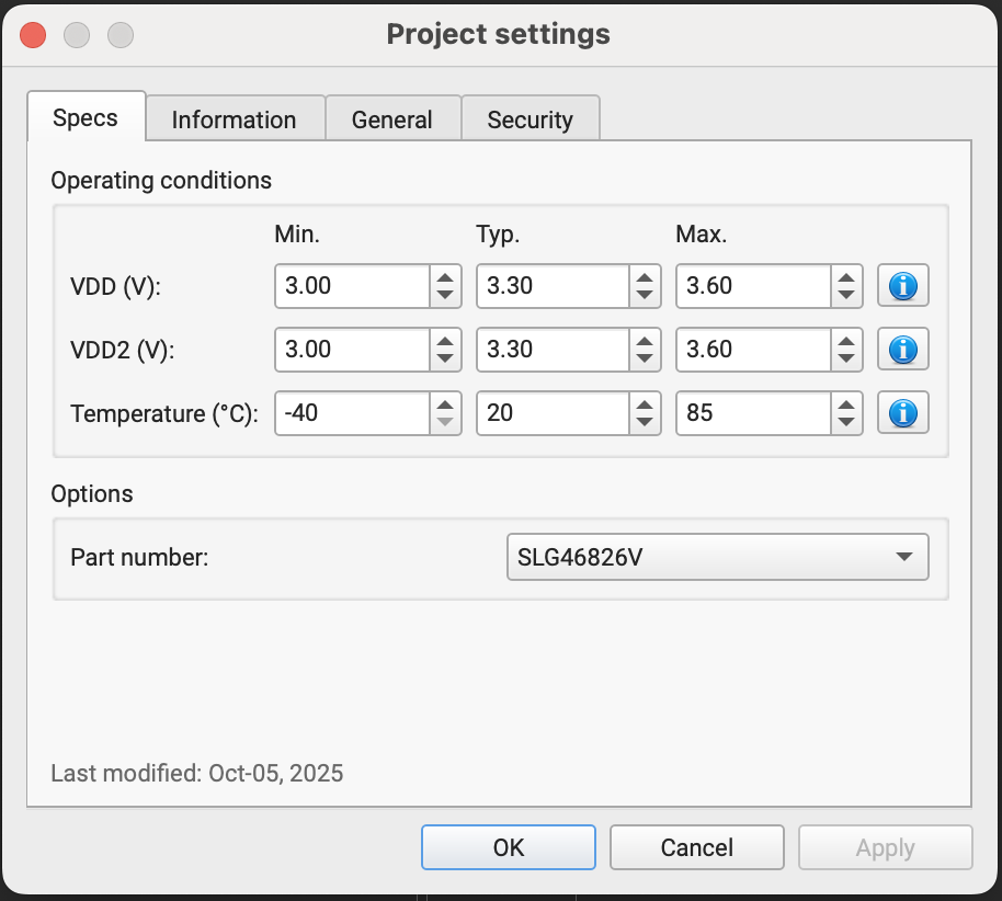
2. After the project window opens up, set the following values for the default operating conditions:
Configuring the I/Os
Enable the following components and double-click each one to modify their properties on the left-hand side.
- PIN3 → RESET_1
- I/O Selection: Digital Output
- Output Mode: 1× open-drain NMOS
- Resistor: Floating
- (Optional) Label the port RESET_1 and flip horizontally so the arrow points right.
- PIN4 → RESET_2
- I/O Selection: Digital Output
- Output Mode: 1× open-drain NMOS
- Resistor: Floating
- (Optional) Label RESET_2, flip horizontally.
- Enable OSC0
- Control pin mode: Power Down
- OSC power mode: Force Power On
- Clock selector: OSC
- Frequency: 2.048 kHz (default)
- ‘CLK’ predivider: 1 (we’ll divide inside delays)
- CNT/DLY for RESET_1 (≈2 s)
- Block: MF0 → CNT/DLY → Mode: Delay
- Counter data: 511
- Edge mode: Rising
- DLY IN init: 0
- Output polarity: Non-inverted
- Clock source/divider: OSC0/8 (~256 Hz)
- Enable/Start: tie DLY_IN to POR (or VDD if you prefer immediate start)
- OUT → PIN2 (RESET_1)
- CNT/DLY for RESET_2 (additional ≈8 s, ~10 s total)
- Block: MF1 → CNT/DLY → Mode: Delay
- Counter data: 39 (with a lower clock)
- Edge mode: Rising
- DLY IN init: 0
- Output polarity: Non-inverted
- Clock source/divider: OSC0/512 (~4 Hz)
- Enable/Start: POR
- OUT → PIN3 (RESET_2)
- POR: Just enable this
You will need to hook all these components up to look like the following schematic:
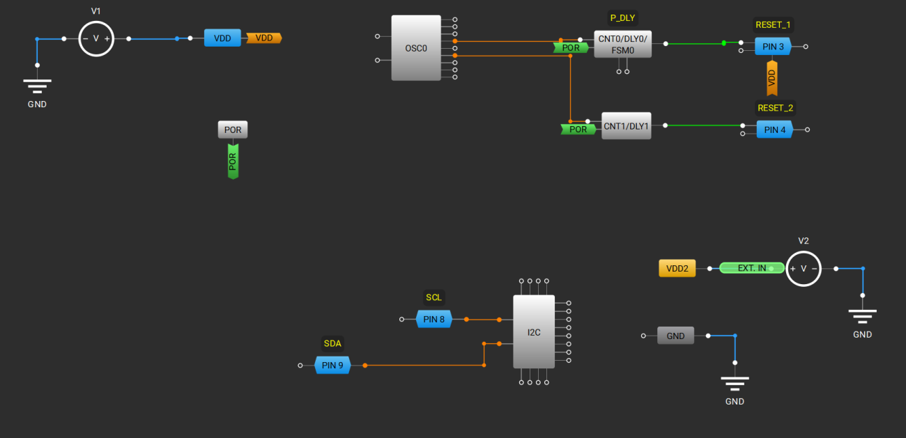
You will notice that there are other components on the schematic, such as extra pins. You can uncheck them in the component box as they are not being used. I’ve also flipped the pin ports horizontally so the wires line up.
Simulating the Design
Click on the Debug button and select Software Simulation. Add probes by right-clicking on a pin of a component and click on Add Probe. I added probes to the clock input of the delay counters, the output of the delay counters, and the external output of the pins. Set your simulation Ending Time (Debugging Controls Panel on the right) to 12s and click on Start Simulation. You should see the /8 clock running much faster than /512, with two clean rising edges: first around 2 seconds (RESET_1) and second around 10 seconds (RESET_2). If the edges aren’t where you expect, tweak the counter data or clock divide values and rerun.
Running in Test Mode
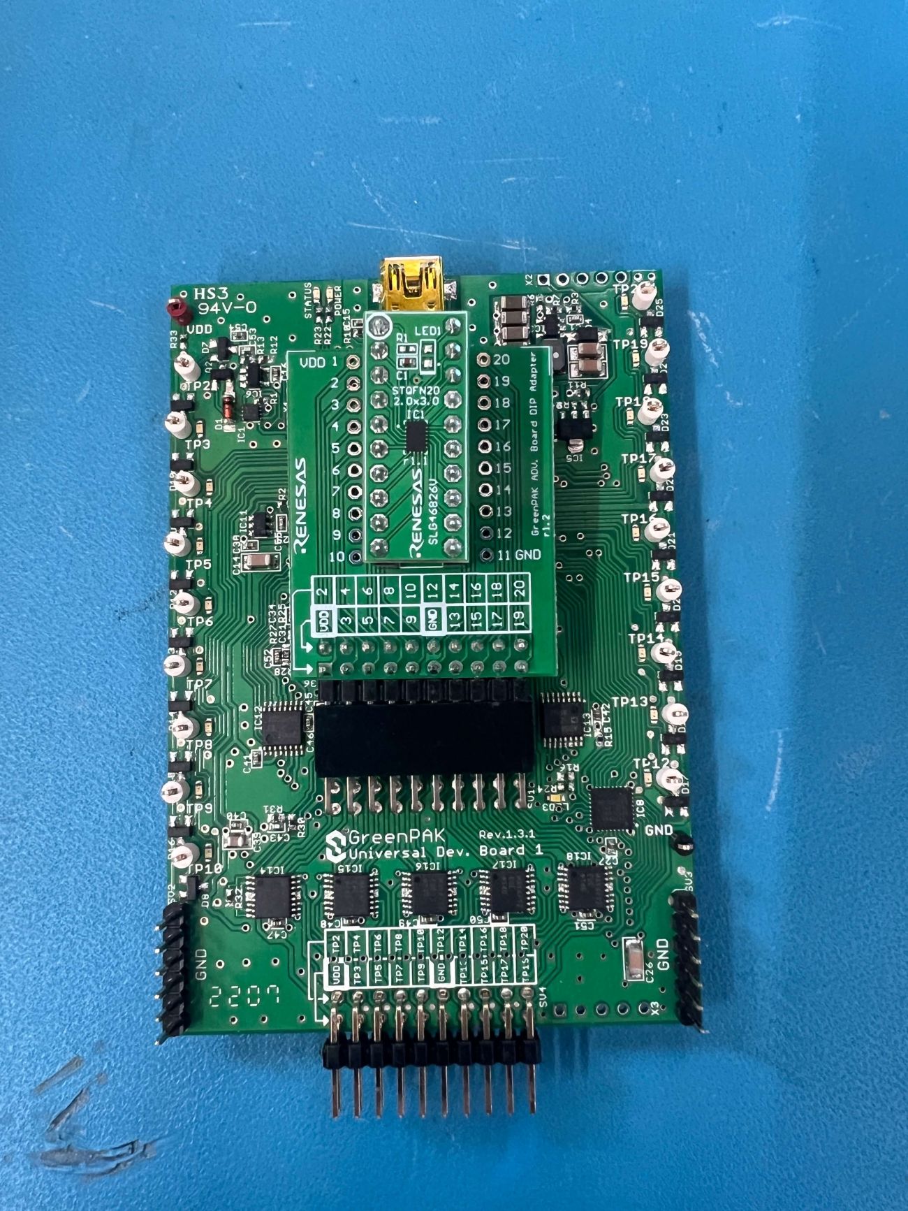
Before you wire the target, use the GreenPAK Advanced Development Platform to visualize timing by running the following:
- Click on the Debug button > Change Platform > GreenPAK Advanced Development Platform.
- Click Test Mode and route the two delay outputs to on-board LEDs by hovering over them and clicking on LED.
- Click on the Program button on the right side and watch TP3’s LED turn on at ~2 s and TP4’s LED ~8 seconds later.
Drop-In on the Target (Two ATmega328P Boards)
Once timing is validated, place the SLG46826V DIP adapter on the breadboard with these two ATmega328P targets:
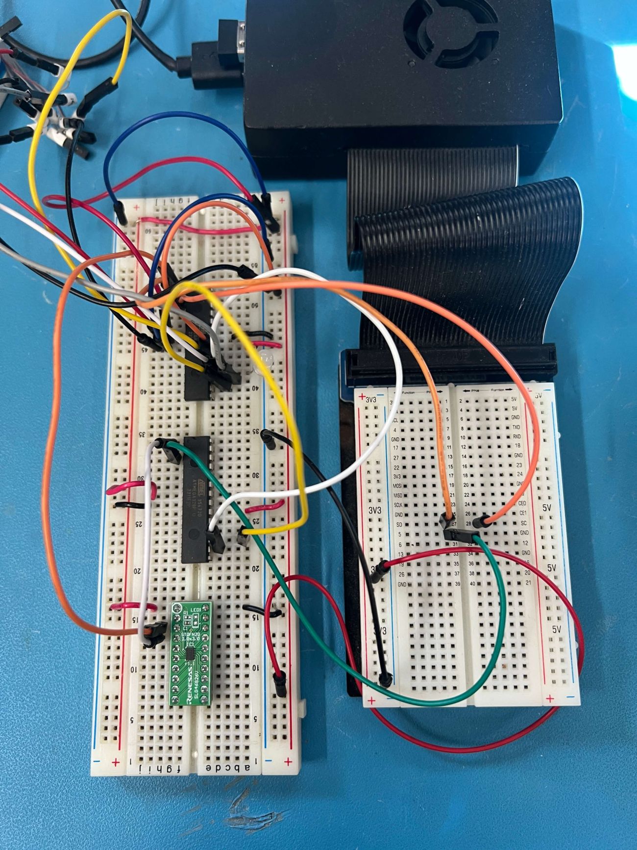
Connect RESET_1 (Pin 3) to the coordinator ATmega’s RESET pin (pin 1); RESET_2 (Pin 4) to the follower’s RESET (pin 1). Make sure to share grounds and supply rails. You can power from a lab supply or a stable 3.3 V source (I used a Raspberry Pi 3.3V source for convenience). Since we’re logging serial, you’ll see the first MCU boot, claim the role, and the second MCU join after the programmed delay (which follows the example demo in Shrinking Arduino Projects: Atmega328P and Nothing More).
Conclusion
In this article, we automated boot sequencing of devices using the GreenPAK SLG46826V chip. While this was a trivial example, it demonstrated the ability to minimize external circuitry or extra microcontrollers to perform tasks such as power sequencing. Using the GreenPAK suite of devices opens up the possibility of performing significantly more complex operations in a single, programmable IC.
Check out the rest of the possibilities on the GreenPAK Programmable Mixed-Signal product page.
About Author
Related Resources
Related Technical Documentation
Table of Contents
Design to Release, Without the Friction
- Keep reviews tied to the right version
- Reduce handoff confusion and rework
- Spot sourcing and release risk earlier
- Work solo, share when needed
Get Started
Thank you, you are now subscribed to updates.