Benefits of Using an Integrated Design Environment for PCB Development

At a Glance
Learn how an integrated design environment reduces friction in PCB development. See how connected data improves collaboration, cuts rework, and accelerates releases.


Most electronics teams do not lose time because their individual tools are inadequate. They lose time at the boundaries between tools. The handoff between schematic capture and layout, the translation between ECAD and MCAD, the reconciliation of BOM data against procurement systems, and the manual synchronization of design files across review cycles all introduce friction that accumulates across every project.
This friction is easy to underestimate because it rarely appears as a single large failure. It shows up as repeated small delays: a connector footprint that does not match the mechanical enclosure, a component substitution that was approved in procurement but never updated in the schematic library, or a design review conducted against an outdated output file. Each of these is individually recoverable, but collectively they extend schedules, increase rework, and erode confidence in the design data.
Key Takeaways
- An integrated design environment helps electrical, mechanical, and sourcing teams work from the same design data.
- Better visibility into requirements, design files, and BOM data can reduce avoidable communication delays and rework.
- Real-time access to current design and supply chain information helps teams catch issues earlier.
- Good tools should reduce manual overhead so engineers can spend more time designing and less time reconciling data.
1. Teams Work From the Same Design Data
The most common integration gaps in hardware development fall between domains that are tightly coupled in the physical product but loosely coupled in the toolchain. Electrical and mechanical design is the most obvious example. A board outline, connector placement, or keep-out zone that is defined in one tool and manually transferred to another creates an opportunity for mismatch every time either side changes. When that mismatch is caught at prototype assembly rather than during layout, the cost is measured in weeks and fabrication dollars.
Component data creates a similar problem. When schematic symbols, footprints, 3D models, and supplier data are managed in separate systems, the designer is forced to verify consistency manually. That verification is tedious, error-prone, and repeated across every new design. The engineering risk here is not that the data does not exist, but that it is not connected to the point of decision. A designer selecting a voltage regulator should see its availability status, package geometry, and thermal characteristics in context, not in a separate spreadsheet that may or may not reflect current conditions.

2. Feedback Moves Faster
In disconnected workflows, feedback often depends on file exports, screenshots, PDFs, and email chains. That slows everything down, especially when teams are spread across time zones or working with outside manufacturers.
A more integrated workflow makes it easier for collaborators to view the latest design, comment in context, and raise questions earlier. Instead of sending files back and forth, teams can respond closer to the design itself.
That shortens the feedback loop and reduces the chances of acting on outdated information.
3. Supply Chain Issues are Easier to Spot Earlier
BOM quality affects schedule just as much as layout quality.
When part data is managed manually, availability, lifecycle status, pricing, and alternates are easier to miss or harder to keep current. That increases the risk of finding sourcing problems late, when the design is already close to release.
An integrated environment with live supply chain visibility helps surface those issues earlier. Engineers can review part status while designing rather than treating sourcing as a separate task at the end. That is especially useful for smaller teams where the same person may be responsible for design, review, and release preparation.
4. Better Visibility Can Reduce Avoidable ECOs
Many ECOs are not caused by design errors. They result from information that was available somewhere in the organization but was not visible to the designer at the point of decision. A mechanical clearance issue, a connector orientation conflict, a packaging constraint, or a sourcing limitation that should have been caught earlier can each trigger a formal change after layout is complete.
When electrical, mechanical, and component data are fragmented across tools, those problems are more likely to surface after decisions have already been committed. Integration reduces this risk by making relevant constraints visible sooner, while the design is still easy to change. The cost difference between adjusting a constraint during schematic capture versus issuing an ECO after fabrication release is typically an order of magnitude or more in both time and dollars.
5. Engineers Spend Less Time Managing Tools
A fragmented workflow creates a surprising amount of administrative work.
Time goes into exporting models, updating spreadsheets, confirming versions, cleaning up libraries, checking whether part data is current, and repeating information across tools that do not stay in sync. None of that is the core engineering problem, but it still consumes engineering time.
A stronger design environment does not eliminate complexity, but it can reduce the amount of manual coordination required to keep the project moving.
That matters because every hour spent reconciling tools is an hour not spent designing.
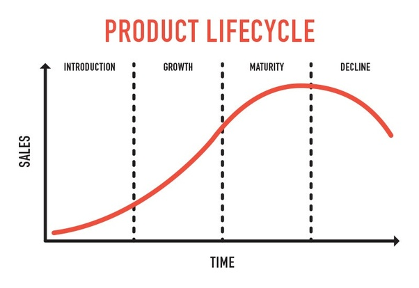
6. Design Data Becomes Easier to Manage Across the Product Lifecycle
The gap between design tools and product data systems creates its own category of friction. Design files are difficult to review without downloading them into the originating tool. Library and part data drift out of sync. Release processes depend on manual coordination between systems that were never built to interoperate. The result is more overhead than visibility, particularly during review, release, and manufacturing handoff.
An integrated design environment improves this by keeping design data and supporting documentation connected throughout the product lifecycle. That does not solve every PLM challenge, but it reduces the friction between designing the board and managing the information around it. For teams that release multiple revisions or manage product families, this connectivity compounds in value over time.
Common Concerns
Our team is already used to its current tools.
That is a real consideration. But the right comparison is not comfort versus discomfort. It is whether the current workflow creates enough drag that the cost of staying the same is higher than the cost of improving it.
We do not necessarily need cloud tools.
The real question is not cloud for its own sake. It is whether your team has timely access to the information it needs without waiting for exports, email attachments, or manual updates.
Will this actually save time?
That depends on where the current delays are coming from. If the team spends significant time on handoffs, file management, BOM cleanup, or chasing design context, better integration can make a measurable difference.
The Bottom Line
The value of an integrated design environment is not that it looks more modern. It is that it reduces avoidable friction in a process that is already hard enough.
PCB development depends on connected decisions. Electrical, mechanical, sourcing, and release information all affect whether a board moves forward cleanly or turns into rework. When those inputs are fragmented across disconnected tools and messages, problems surface later than they should.
Integration helps by making the right information easier to see, easier to share, and easier to act on while the design is still flexible.
Altium Agile Teams brings this level of integration to growing and distributed hardware teams by providing a shared environment where design data, BOMs, reviews, and revisions stay connected. Instead of relying on file exports, spreadsheets, and side‑channel communication, teams work from a common source of truth that keeps electrical, mechanical, and sourcing decisions aligned as designs evolve.
By making the latest design context visible to everyone involved—designers, reviewers, procurement, and manufacturing—Agile Teams helps surface issues earlier, reduce avoidable ECOs, and shorten feedback loops. Design reviews happen in context, BOM changes are easier to track, and release preparation becomes more predictable because everyone is working from the same verified data.
Rather than adding heavy process or enterprise overhead, Altium Agile Teams focuses on reducing the friction that accumulates between tools, roles, and project stages, so teams can spend less time reconciling information and more time moving designs forward with confidence. Get started with Altium Agile Teams today →
Frequently Asked Questions
What is the difference between an integrated environment and multiple tools that export to each other?
Export-based workflows can work, but they introduce gaps where files become outdated, handoffs take longer, and context is easier to lose. An integrated environment reduces that dependency on manual transfer.
How do I know if my current tool stack is costing time or money?
Look at revision cycles, time spent on file management, BOM cleanup, clarification loops, and late-stage changes. If those are recurring pain points, the workflow is likely contributing to the cost.
What if my team works across time zones?
That usually makes integration more valuable, because shared visibility and in-context feedback reduce the need for synchronous communication.
Do we need to replace everything at once?
Not necessarily. Many teams start by improving the area with the most friction first, such as design review, BOM management, or ECAD-MCAD coordination.

About Author
Related Resources


Table of Contents
- Key Takeaways
- 1. Teams Work From the Same Design Data
- 2. Feedback Moves Faster
- 3. Supply Chain Issues are Easier to Spot Earlier
- 4. Better Visibility Can Reduce Avoidable ECOs
- 5. Engineers Spend Less Time Managing Tools
- 6. Design Data Becomes Easier to Manage Across the Product Lifecycle
- Common Concerns
- Our team is already used to its current tools.
- We do not necessarily need cloud tools.
- Will this actually save time?
- The Bottom Line
- Frequently Asked Questions
- What is the difference between an integrated environment and multiple tools that export to each other?
- How do I know if my current tool stack is costing time or money?
- What if my team works across time zones?
- Do we need to replace everything at once?
Speed at Scale. Structured Repeatability. Secure Flexibility.
- Start up fast with out‑of‑the‑box workflows
- Collaborate using ECAD‑MCAD codesign tools
- Manage BOMs with live supply chain part data
- Manage access and security as teams scale
Contact Us
Thank you, you are now subscribed to updates.