Modeling and Placing PCB Connectors Within Altium Designer

ALTIUM DESIGNER
The most powerful, modern, and easy-to-use PCB design tool for professional use.
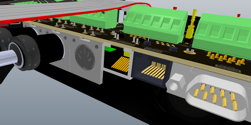
I/O use connectors for PCB system integration
In this guide to PCB connectors, we’ll take a look at connectors within electrical systems, how they benefit from ECAD/MCAD tools, and optimal design specifics like appropriate cable connectors or gold fingers gold plating.
Connectors abound on printed circuit assemblies given integrated electrical equipment and their internal electronics. Now decades into digital systems data is flying across the room and across the world’s communication needs. Protocols for input and output like universal serial bus (USB) and Ethernet all require physical electro-mechanical connectors between equipment and their printed circuit assemblies.
Building connectors onto printed circuit assemblies requires definition of communication channels in both ECAD and MCAD modeling tools. Defining communication channels informs connector component selection. With chosen components comes footprints with land patterns and housing dimensions for the conductive materials of the connector. This ensures, for example, appropriate use of gold plating on gold fingers or smart terminal and pin placement in the printed circuit board PCB design.
Altium Designer provides libraries containing thousands of connector styles along with footprints and 3D models. Footprint editors allow addition of the latest and greatest connector offerings by vendors as well. The unified environment imports, as well as exports, .STEP files for easy sharing with mechanical designers. Ease of collaboration drives elegant designs for IO within your design.
Printed Circuit Board Connector Use Within Electrical Systems
Connectors in electrical design provide connection for signals traveling either into or out of, the printed circuit assembly. They are some of the larger electro-mechanical components on a printed circuit assembly. Used to house conductive pin for connections to pads on the circuit board that interface input-output (IO) signals with other equipment within the system. Connectors have two parts to enable attachment from your PCB to other PCBs, cables, or devices within an electrical system. Whichever connector is used on the PCB must mate with its intended connection point on system devices.
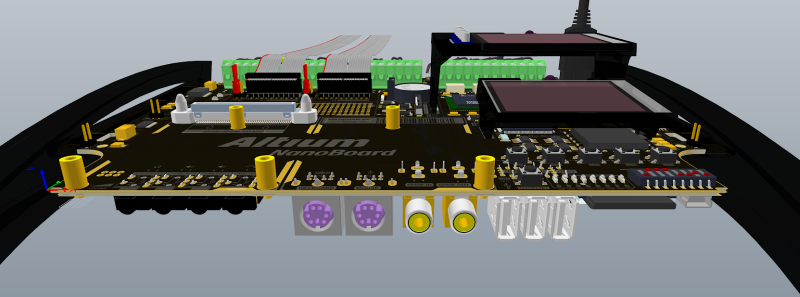
Observe connector placement on your PCB with 3D modeling
Connectors enable Input and Output on PCBs
Connectors are specified in pairs, one a plug, the other a socket. Mechanical features to consider are size, materials, and locking mechanisms. Electrical characteristics to consider are insulation between pins and contact resistance at connection points. Connectors are categorized by the type of signal propagation in terms of input and output. Standards for USB, RS-485, Ethernet, MIDI, SVGA, HDMI, and Radio Frequency resolve into standard mechanical design offerings in connectors. There are thousands of connectors in use for electronic signal transmission. Those best suited for use on PCBs are surface mount connectors, although many through-hole connectors are used on PCBs for both robustness and for the ability to make solid ties to internal grounding planes.
- PCBs have many types of IO connectors
Incorporate function with Sporty 3D Component Model Drivers for Layout
- Memory PCB design pads plug into motherboard sockets
Consider protocol for memory before designing PCB connection interface
- USB is a universal protocol for connecting devices and there are new developments
Compare USB Type-C: A New Frontier for Power and Data Transmission
Defining IO for your design informs selection of components to put into your 3D model.
Connectors Benefit from Compatible ECAD/MCAD Tools
There are many connectors for IO interface to join PCB connector signals to other devices. Considering types of IO utilized by the circuits on your PCB drives selection. Through-hole connections benefit from grounding shields and pins. Grounding pins that travel through the PCB can be tied off to any, or all, of the ground planes in the PCB layout. Noise from IO connections can be directed to ground planes which create pathways to the case part. These direct paths keep noise away from critical signals. Surface mount connectors are lighter and are suitable for low-power connections when onboard grounding schemes are adjacent to routed nets.
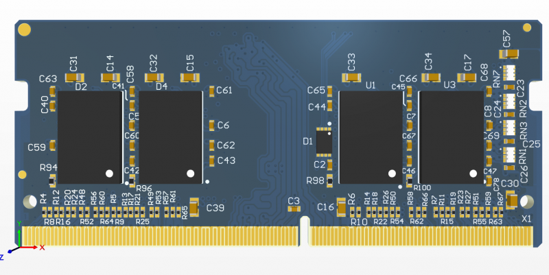
Memory sticks incorporate pad plugs for connections to motherboard receptacles
Use 3D modeling to Make and Place Connectors for IOs
Both through-hole and surface-mount connectors are found in component libraries or may be added by consulting vendor datasheets. Thoughtful placement onto the PCB for electrical and mechanical design considerations is useful in meeting design requirements. Distance between pins and type of insulation material within the connector are worthy of analysis for prevention of arcing. Added impedance to traces at the connection is worthy to note for effects on signal integrity during transmission. Form and fit within the intended space bears consideration by mechanical engineers to ensure keepout violations with confined case parts. Using modeling tools portable across ECAD and MCAD environments expedites design resolutions before going into manufacture.
- Place connectors with powerful tools incorporating MCAD modeling
Unite with a 3D PCB Editor that Simplifies Concurrent ECAD/MCAD Modeling
- Find thousands of component models in database libraries
- Connect IOs on your PCBs using buses
3D modeling is made easy with EDA tools designed to accommodate their use.
Altium Designer Incorporates Powerful Tools for Connections
Altium Designer has a large toolset to accommodate connector modeling and placement. It begins with component libraries containing many of the connectors commonly found on PCBs for USB, RS-485, Ethernet, MIDI, SVGA, HDMI, and more. Using library parts to place connectors onto the PCB is easy.
In addition, Altium Designer provides a friendly printed circuit board design environment for porting both ECAD and MCAD files both into and out of the other’s modeling tools. Such collaboration enables easy modeling for keepouts and avoids collisions when going into manufacture. Further, Altium Designer provides accessible workspaces for multi-board development. Interfaces may be studied for alignment and evaluated for signal propagation across multiple boards. The workspace allows 3D rendering while moving parts during design refinement to ensure optimal cabal connections, such as USB or coaxial connector ports.
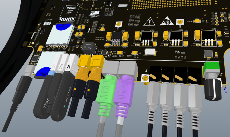
Altium’s 3D environment allows cable attachment to your onboard connectors
Altium’s Mighty ECAD/MCAD Partnership Benefits Connector Placement
Rather than memorizing a detailed guide to PCB connectors, you can focus on the task at hand by choosing Altium Designer for connector development that evaluates transmission effects at connector interfaces. Using integrative EDA tools allows components development with the libraries before placing onto the PCB. After placement on the PCB collaboration with MCAD models is easy with .STEP file export and import. Using .STEP files facilitates mechanical engineering evaluations for PCB fit into case part enclosures.
- Evaluate mechanical alignment of printed circuit board connectors with compatible MCAD
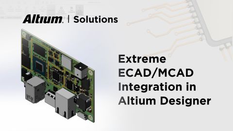
See how 3D works within Altium Designer with MCAD Integration
- Build connector land patterns and footprints for 3D modeling
See how the Altium builds and stores 3D connector IPC Compliant Footprints
- Get Altium’s Solidworks PCB connector to integrate your IOs
Find how to get real-time support with Solidworks PCB Connector
- Evaluate input-output connections across multi-board assemblies
Take a look at 3D connection modeling in Altium’s unified environment
Get your printed circuit boards connected with Altium Designer’s unified environment to support IO requirements for your PCB assembly. Using integrated tools to evaluate signal integrity and collision checks at IO connections promotes success on your first pass production designs.


