


Part 3: Documenting Your PCB for Assembly

At a Glance
Learn everything you need to know to have you board successfully assembled, including assembly drawing requirements, adding notes, and cautionary markings.


With your fabrication (bare board) requirements documented, it is now time to move on to an equally important stage — documenting the instructions for component placement and final assembly. It is in the assembly stage where your bare board is brought to life with all the components you specify in your Bill of Materials. This chapter will cover what you need to know to have your board successfully assembled and will cover assembly drawing requirements, adding notes, and placing cautionary markings.
If you would like to skip to different chapters in this series, use the Table of Contents links below:
- Setting Up Your Fabrication Document
- Documenting Your Master Drawing
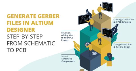
- Creating Fabrication and Assembly Drawings In Altium Designer
Required Assembly Documentation
The required assembly documentation consists of a number of assembly drawing templates that you will need to include with your final design including schematic prints and a finalized BOM. In addition to your notes, these drawing templates will allow your manufacturer to clearly understand your design intent for final component placement and assembly.
Assembly Drawing Requirements
Your design documentation is the most important aspect of your design. Even the greatest PCB design will go to waste, if you are not able to clearly communicate design intent to your manufacturer and your project stakeholders. With your master drawing completed, you now have everything you need to get a bare board produced by your chosen fabricator. In the next chapter we will explore the last piece of the documentation puzzle for the final assembly of your PCB.
An example assembly drawing from my NFC reader project is shown below. This assembly drawing shows the expected locations of components in the assembled board on the top side and the bottom side. This is not meant to be a replacement for pick-and-place data, but rather it provides a visual check with which a PCBA can be checked post-assembly.
What is more important in the assembly drawing is the assembly notes, which include important requirements on the PCBA, such as:
- Soldering requirements (solder type, composition, etc.)
- Inspection requirements
- Handling and packaging requirements
- RoHS compliance
The assembly notes are kept distinct from the fabrication notes because they are only needed during the PCB assembly process.

Bill of Materials
The Bill of Materials will include a detailed and sourceable part list that includes all necessary part supplier information. Providing a BOM to your manufacturer with included component designators and supplier information ensuring your design will be manufactured with the appropriate parts. The BOM is covered in depth later in the guide. The drawing sheet below shows a sample BOM with some of the necessary part information you will want to include:

Cautionary Markings
Cautionary markings are very important for safe handling of your board. As part of your assembly documentation, you will need to include the electrostatic discharge markings shown below if your board requires special handling due to static sensitivity.

In addition to the symbols above, the notes in the table below need to be placed above or as close to the title bar as possible. The notes used depends on the class of your board, and markings can be applied using copper etching or silk screening.
| |
Notes
Assembly drawings, like fabrication drawings, require their own set of notes. These notes include information about the merging of the board with its components, including assembly standards, handling instructions and solder specifications. There’s no such thing as too much detail in your assembly documentation. If you think your manufacturer needs to know something about a specific component’s placement or assembly requirements, make a note for it. Below are some examples of assembly notes as seen in IPC-A-325A[8-1]:
- Workmanship to be equal to and compliant with the requirements of IPC-A-610.
- Mark group (or dash) number, revision and serial number as shown; marking to be 0.10’’-high characters using item no. 6, white epoxy ink, per MILI-43553, type II.
- This assembly contains electrostatic discharge (ESD) sensitive devices; static-free handling is required per MIL-STD-1686, class 2
- Conformal coating is not required.
- Designations are for reference only and do not appear on individual parts.
- Dimensions shown specify maximum envelope limits for the finished assembly.
- Orientation of polarized capacitors is denoted by a plus (+) sign. Polarity is identified on the part.
- Dot identifies pin #1 location and device orientation when viewed from the top.
- Using solder paste screen, apply solder paste, item #4, to primary side of board.
Completing Your Design Documentation
Draftsman is a sophisticated yet easy to use drawing tool that is integrated within Altium Designer, for the creation of fabrication and assembly drawings. Draftsman is a built-in extension that can be installed or removed manually by going to the Extensions and Updates page. You can access the Extensions and Updates page by clicking on the user icon on the top right of the Altium Designer window.
The next time you need to create fabrication documents for your PCB project, use the Draftsman utility in Altium Designer®. This powerful, easy-to-use feature is included in Altium Designer and it will help you speed through the document creation process.

About Author
Related Resources
Related Technical Documentation
Table of Contents
Design to Release, Without the Friction
- Keep reviews tied to the right version
- Reduce handoff confusion and rework
- Spot sourcing and release risk earlier
- Work solo, share when needed
Get Started
Thank you, you are now subscribed to updates.


