


DC Power Integrity: 5 Common Myths


Power integrity is nothing new, but it is becoming more and more of a concern in power electronics, particularly high-current DC/DC converters. With the continuing trend of faster and smaller products, we no longer have the luxury of space. Each millimeter is precious, and we need to design that way. If you’ve been in the industry for more than a few years, you may have heard many of the following PI myths.
Myth 1: Throw Copper at It
You may have been told that the more copper, the better. And by simply doing a copper pour or using higher copper weight, you can solve most if not all of your problems as they relate to DC power integrity. This, of course, is not the case; you may be able to solve some heat issues, but you also invite other problems such as the creation of islands and peninsulas. Although they seem harmless, islands and peninsulas have specific resonant frequencies, which could cause failures when certain conditions exist. These failures may appear random and are thus extremely difficult to pinpoint and fix. So before you blame it on black magic or some sort of voodoo, make sure to check if your copper pours are creating islands or peninsulas, because you don’t want to toss your design away and redo your layout.
However, if you already have a multi-layer board with high layer count, adding more power layers at low copper weight is always better than increasing the copper weight. This is especially true for power on the surface layers; it will be better to add a plane layer inside the stackup. The reason for this is that the additional cost will be marginal and it can have little to no impact on the rest of the design unless the stackup gets excessively thick. Even in the case of an overly thick stackup, the only parameter that changes is the via aspect ratio limit.
Myth 2: Stick to IPC-2221/IPC-2152
This one might come as a surprise to you as it does with many others. Yes, IPC-2152 is important and provides guidance on how to avoid issues by means of minimum trace widths for acceptable temperature rises. Applying IPC-2152 in this manner forces the designer to allocate more space than necessary to your PDN, taking up valuable real estate or even creating more layers for a design.
IPC- 2152 is a great tool to have at your disposal and should be well understood if you want to make the most efficient power delivery designs, but it shouldn’t be blindly applied. Engineers who use IPC-2152 in a more thoughtful way alongside a power integrity tool can reduce their power distribution network area while still ensuring a safe design goes out for production.
The other possible standard to use for copper sizing and thermal management is IPC-2221. This standard is a generic design guidelines standard and it provides guidance on trace width sizing that precedes the guidance found in IPC-2152. With two standardized options available, which of these standards should you use to size traces and power rails?
IPC-2152 supersedes the trace sizing charts in IPC-2221 and should be the preferred reference for current-carrying capacity calculations. The older IPC-2221 charts were derived from a limited dataset collected in the 1950s and are known to produce inaccurate temperature rise predictions, particularly for conductors on internal layers and wide power rails. IPC-2221 tends to underestimate temperature rise for internal traces because the original test data did not adequately account for the reduced convective cooling available to buried copper. IPC-2152, by contrast, is based on a much larger and more modern experimental dataset and provides correction factors for board thickness, copper weight, and proximity to planes.
The major differences include:
IPC-2221 uses a single set of curves for internal and external layers with limited empirical backing, while IPC-2152 provides separate, experimentally validated curves with additional derating factors.
IPC-2221 can underpredict temperature rise on internal planes by a significant margin, leading designers to undersize rails that lack direct convective cooling.
IPC-2152 accounts for the thermal coupling between layers and the effect of adjacent copper, giving more realistic predictions for multilayer stackups where power planes are buried.
IPC-2221 does not address the effect of board thickness or total copper area on heat dissipation, both of which IPC-2152 incorporates through empirical correction charts.
Myth 3: You Can Never Have Too Many Vias
The narrative about vias is the corollary to the narrative about copper, namely that more vias always gives better results. In reality, this is not always true in DC power electronics. There are two reasons we want to make smarter use of vias when connecting rails carrying high current:
- Vias can cut up plane layers.
- Eventually, each new via will produce a smaller impact on heat transfer.
The first point means that you are adding current carrying capacity on one circuit or interconnect, but you might be reducing it in another area of the design. For example, if you have a power layer with very large rails, and you need to drill your vias through it, you're turning that rail into Swiss cheese, reducing its current carrying capacity.
The image below shows what happens in a power rail (left side of the image) when too many vias are placed too close to each other: the drill creates large voids in the power rail during fabrication, which reduces its current carrying capacity.
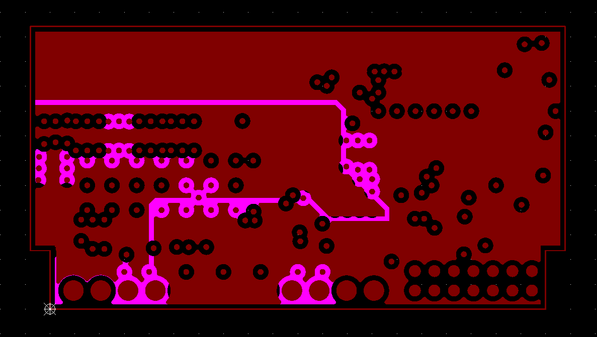
If you are well versed with IPC-2152, you may have noticed that they are quite loose when it comes to vias. Like with trace width, IPC-2152 is very conservative and may leave your board with larger and more vias than necessary. This can be a problem when your copper shapes are now perforated with large holes. What this does is decrease the area available for the current, which increases the current density and consequently, the temperature. Not only that but it also takes away real estate from the rest of your design, making it especially challenging and time-consuming to finish routing that last 10% of your board. As with the other IPC-2152 rules, take them into account and understand them but don’t just blindly follow.
The second point is important in relation to heat transfer, which is one of the reasons we study DC power integrity in the first place. When DC power dissipation occurs, it causes the copper to heat up, thus giving us guidelines in the IPC-2221 and IPC-2152 standards.
The impact of vias on heat transfer has been studied by PCB simulation expert Dr. Johannes Adam and industry legend Douglas Brooks. They found that a surprisingly small number of vias gets you extremely close to the theoretically minimum thermal resistance condition when vias are used to connect large sections of copper. This surprising result goes against footprint guidelines sometimes found in datasheets, where an IC manufacturer might recommend a dozen or more thermal vias be placed on the die attach pad of a relatively small and low-power integrated circuit.
To learn more about this, watch the video below on the Altium Academy YouTube channel.
Myth 4: Copper is Copper
Not all copper is created equal, and we often overlook this. A small and commonly neglected factor when analyzing a power distribution network is the conductivity of copper. As stated before, not all copper is equal. The conductivity of PCB copper is different than the conductivity of pure copper and therefore analyzing your design with a different conductivity can give you drastically different results. We’ve found that on average the conductivity of PCB is 4.7e7 S/m while pure copper 5.88e7 S/m. That's a 22.3% difference! You should always check with your manufacturer for clarification on this important variable.
Copper has non-zero resistance, and this finite conductivity means that different components in a circuit will experience different levels of power dissipation depending on the length and cross-section of their current paths. Consider FETs in a driver circuit as a practical example. Depending on how the FETs are arranged and connected with copper, some FETs may see a longer current path from the supply rail through the copper channel to the load. The additional resistance in that longer heat causes other devices to run at higher current than intended, potentially exceeding their current rating. This asymmetry is a direct consequence of the layout geometry and copper pour design.
This is why we use a PDN analyzer: to map out current paths and find regions with high power dissipation. The power dissipation found in these regions can inform where to add more copper or how to change the component arrangement so that heating is more uniform. This can help prevent hot spots in the design or even prevent component failure due to thermal stresses.
To learn more, watch the Altium On Track podcast episode below, featuring Caleb Buck.
Myth 5: You Need to Be a Simulation Expert
It used to be true that you needed to be (or know) an expert to perform power integrity analysis. Many times you would have to export your design to a power integrity or simulation expert because the software used is too intricate and loaded with different options and parameters. This is not an ideal solution, not even close. It’s expensive, takes a lot of time and you’re going to have to export and import many times until your board is finally done.
With today’s designs so small, and consumers expecting so much, we can’t avoid power integrity analysis any longer; it's a must-have for modern products. Remember, copper doesn’t solve all your problems, vias aren’t as friendly as we thought, and IPC=2152 isn’t absolute truth but more of a jumping off point.
What you really need is an easy to use tool that's integrated with your current design software, which visually shows you the issues and allows you to make changes during design time. That way you don’t need to constantly go back and forth with your simulation guru.
Whether you need to build reliable power electronics or advanced digital systems, use Altium’s complete set of PCB design features and world-class CAD tools. Altium provides the world’s premier electronic product development platform, complete with the industry’s best PCB design tools and cross-disciplinary collaboration features for advanced design teams. Contact an expert at Altium today!
About Author
Related Resources
Related Technical Documentation
Table of Contents
Design to Release, Without the Friction
- Keep reviews tied to the right version
- Reduce handoff confusion and rework
- Spot sourcing and release risk earlier
- Work solo, share when needed
Get Started
Thank you, you are now subscribed to updates.

