Reverse Engineering Project Libraries

Outsourcing has become the de-facto solution for companies seeking to cut costs and increase their profit margins. Rather than consuming their own resources on a particular task, companies farm it out to other firms that specializes in that particular area, leaving them to focus on what they do best. New product design often gets contracted out to separate design firms. If that’s you — your company outsources PCB design or your company is a PCB design house — read on because this paper can make your life easier.
COMMUNICATION
Outsourcing work to other companies demands better communication among all parties involved. For PCB design services engineers, this means ensuring that complete Printed Circuit Board project files are sent to clients. Unfortunately, receiving PCB or gerber files from clients isn’t always as smooth a process. Clients may send incomplete project files, project files with unstandardized component libraries, or other files that don’t match what you actually need. When that happens, how do you proceed with the project? Here is an overview of the challenges that can arise when board designers need to generate source libraries solely from design project files, as well as some available solutions that can help facilitate this process.
PRINTED CIRCUIT BOARD PROJECT FILES
Project file structure varies widely among different brands of PCB design software. Typically software packages have the six file types illustrated in the following table.

Table 1: Typical file structure for PCB design software packages
Most Printed Circuit Board schematic and/or gerber files are self-contained. This means that a PCB design contractor could send just the schematics or PCB file alone to a client, and the client would be able to open and view the full Schematic and PCB file content. This flexibility may seem convenient, but it can be a double edged sword. It often leads to situations wherein a customer only recovers PCB or Schematic files due to premature termination of an agreement with their previous contractor(s). The client’s next contractor then gets burdened with having to base future designs off of the incomplete project files that the client has supplied. Autom
In many cases, editing components within the design is not immediately possible with Schematic and PCB files alone. In those cases, Schematic and PCB library files are required as well. This becomes all too evident when a designer needs to mass-edit components in a PCB design project. With library files, contractors have more flexibility, including the ability to:
- Modify a given component footprint and update thousands of references
- Create standardized components
- Modify component footprints and symbols
Achieving these tasks for a few components is easy. But how about having to recreate a footprint and symbol for thousands of different components, each time a new design arrives from a client? The contractor would need to reinvent the wheel, regenerating new libraries for the existing design. It’s both impractical and incredibly time consuming. The solution is utilizing automated reverse engineering PCB project libraries.
REVERSE ENGINEERING PRINTED CIRCUIT BOARD PROJECT LIBRARIES USING ALTIUM DESIGNER
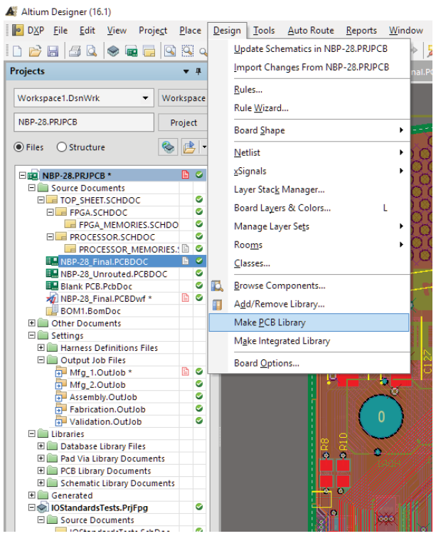
Altium Designer incorporates three separate tools that can make re-engineering schematic and PCB libraries from raw schematics or Printed Circuit Board PCB (SCHDOC and PCBDOC) files much easier. There’s a “Make Schematic library” tool for schematic files and a “Make PCB library” tool for PCB files. Finally, there’s the “Make Integrated Library” tool, to incorporate documents from both file types. Each tool automatically generates source libraries from supplied Schematic and PCB documents with a single mouse click.
As shown in Figure 1, access the “Make Schematic Library” tool from the menu option Design -> Make Schematic Library while a schematic document is active. This PCB design tool generates a library file
containing a symbol and/or SPICE model for each unique component in the design. For components using the same symbol reference, only one library symbol entry is created.

Figure 1: Access to the “Make Schematic Library Tool”.
You can see in Figure 2 that the Make Schematic Library tool can be accessed from the menu option Design Make Printed Circuit Board Library, while a Printed Circuit Board document is active. This tool generates a library file containing a footprint and/or 3D model for each unique component in the design. For components using the same footprint reference, only one library footprint entry will be created.

Figure 2: Access to the “Make PCB Library Tool”.
In Altium Designer, integrated PCB design libraries contain, at minimum, both PCB footprints and their associated Schematic symbols. They can also include SPICE and 3D models of components. The “Make Integrated Library” tool can be accessed from the menu option Design -> Make Integrated Library, while either a Schematic or Printed Circuit Board document is active. This tool generates a library file containing both footprint and symbol information for each unique component in the design. It is essentially a container for Printed Circuit Boards and SCH libraries. Because integrated libraries are read-only by default, they’re perfect for situations where contractors need to send source files to clients for final review, but do not want clients accidentally modifying those files. Of course, integrated libraries can be easily edited if the need arises.
CONCLUSION
The reverse engineering process of PCB project libraries is not an easy task. Depending on how many components are in the PCB design source files that you received from the customers have, reverse engineering could take anywhere from a few minutes for small projects, to several days for larger projects. When contracting PCB design work, wasted time means wasted money, both for the contractors and for the clients. This extra time spent recreating libraries can end up sending both parties over budget. So why spend all of that time and money re-inventing the wheel, when an automated, affordable, and time-saving solution exists with Altium Designer?


