


What Are Molded Interconnect Devices or MIDs?

At a Glance
Discover how Molded Interconnect Device (MID) technology integrates circuits into 3D structures, reducing size, weight, and complexity in electronic designs.


What is the next big thing in design? Is it graphene? Flex? Or maybe something else. If you've been thinking about the future of PCB design, then you may have come across molded interconnect devices or MIDs. In this blog, we’ll explore what MIDs are, and some molded interconnect device uses.
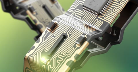
According to MIDIA (Molded Interconnect Devices International Association), a Molded Interconnect Device is an injection molding with plastic, which incorporates a conductive material pattern and integrates both mechanical and electrical functions. It’s the fusion between a plastic part and a copper circuit trace is etched onto the surface of the plastic part, creating tracks and pads which can then house electrical components. What you get is a cool electromechanical piece of hardware. That is an MID.

Where MIDs Are Used and Advantages of MIDs
You can find MIDs across many industries and products, from medical to automotive industries, and on cell phones and tablets. MIDs make sense for these types of industries and products because of the need to have sleeker designs. Sometimes, it’s not practical or possible to have many interconnect components and wires. Phones are a great example of this.
We’re always trying to pack more in a smaller package, so something like a MID can really help us out. By using a molded interconnect device in a phone, we can have the antenna integrated with the mechanical enclosure, saving us space on our board and even giving us a better-functioning antenna. These same principles can be applied to any field, including automotive. Below, you can see MID technology in a car steering wheel, eliminating the need for wire harnesses.
How Are MIDs Made?
Even though the Molded Interconnect Device market has existed for many years, its adoption was initially slow. However, in recent years, MIDs have gained traction in automotive, medical, and consumer electronics industries, thanks to advancements in manufacturing techniques and miniaturization needs.
MIDs will not replace PCBs, but they serve as a valuable complement in designs requiring compact, lightweight, and integrated electronic-mechanical solutions. While there are multiple ways to create MIDs—such as Laser Direct Structuring (LDS), Two-Shot Molding, Metal Spraying, and 3D Printing—LDS has emerged as the most widely used and standardized process, making MID manufacturing more defined than in the past.
Laser Direct Structuring
Laser Direct Structuring (LDS) begins with a single shot molding to create the physical part. Then, a laser etches away a thin layer of plastic where the traces will be. Next comes the metallization process where the plastic part is plated with copper. At this point, you’d have your part go through a 3D pick and place machine where electrical components can be placed.
![]()
Laser Direct Structuring (Based on LPKF Video)
Two-Shot Molding Process
The Two-Shot MID process combines two plastics which are molded together to form a single part. The first resin that is shot into the mold is usually not plated because sometimes processes differ between manufacturers. This first injection forms a base for the second shot to build off of; this second shot is highly plateable.
Next, the plastic mold goes through a chemical treatment to promote the adhesion of copper to the mold. After this process, the plastic are put through an electroless plating process where copper is deposited on the part as copper traces.
Metal Spraying
Metal spraying is similar to laser-direct structuring as it uses the same technique up through the LDS process, but it does not make use of a chemical bath to adhere the copper. Instead, as you’ve probably guessed, it uses a metal spraying technique to deposit the copper on the part. Metal spraying allows for thicker circuitry and also doesn’t need the plastic to be plateable. You may be asking then, how does the metal stick? Well, LDS roughens the surface of the plastic so the metal may easily adhere and stay in place therefore chemical baths are not needed.
3D Printing
An emerging method for MID production is 3D printing, which allows for direct fabrication of conductive traces onto plastic structures without traditional molding or plating steps. Using techniques like Direct Ink Writing (DIW), multi-material extrusion, and laser sintering, 3D printing enables complex, customized designs that integrate electrical and mechanical functions.
Unlike injection molding, this approach offers tool-free production, rapid prototyping, and reduced material waste. However, current limitations include lower circuit density and conductivity compared to traditional methods.
As materials and printing techniques advance, 3D printing is expected to play a growing role in flexible, wearable, and miniaturized electronic applications.
Are MIDs the Future?
MIDs are steadily carving out their place in the future of electronic design. While traditional PCBs remain essential for high-density circuit applications, MIDs offer a revolutionary approach by seamlessly integrating electronic and mechanical functions into a single, space-saving structure.
The technology behind MIDs has evolved significantly, making them more precise, reliable, and scalable. Today, MIDs are being adopted across industries that demand sleek, miniaturized, and high-performance designs, such as automotive systems, medical devices, IoT applications, and high-frequency communications.
While traditional PCBs can support dozens of layers, MIDs excel in applications where flexibility, weight reduction, and space efficiency are critical. They enable innovative designs by embedding circuitry into enclosures, eliminating bulky wiring, and even improving antenna performance.
The growing adoption of MIDs in automotive radar, touch-sensitive controls, wearable technology, and medical implants suggests that this technology is not just a passing trend—it’s a powerful tool for next-generation electronics.
So, will MIDs completely replace PCBs? Not anytime soon. But will they redefine how we design compact, high-performance electronic systems? Absolutely.
Learn More
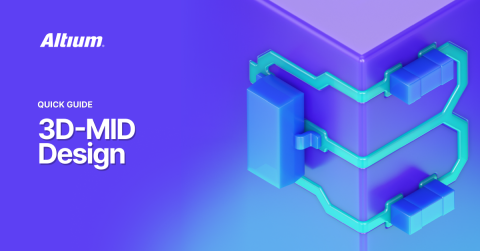
Want to see how MIDs can be designed in a true 3D environment? Check out how Altium supports 3D MID design with advanced visualization and routing tools.

About Author
Related Resources
Table of Contents
Design to Release, Without the Friction
- Keep reviews tied to the right version
- Reduce handoff confusion and rework
- Spot sourcing and release risk earlier
- Work solo, share when needed
Get Started
Thank you, you are now subscribed to updates.