Create high-quality PCB designs with robust layout tools that ensure signal integrity, manufacturability, and compliance with industry standards.
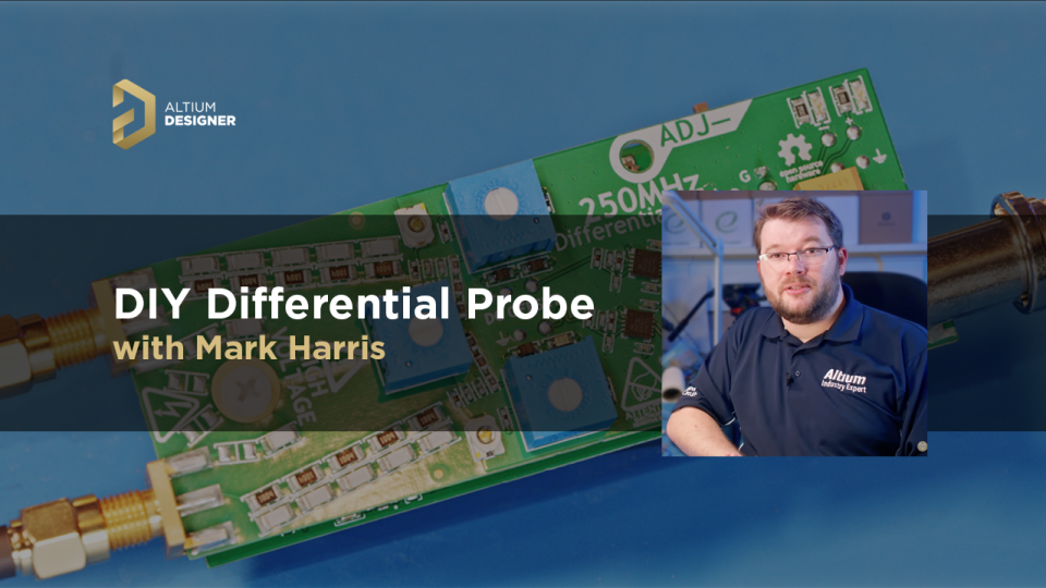
Do you need a differential probe for your oscilloscope? Join Mark Harris designing a DIY differential probe, and exploring the advantages of using a differential probe for testing your circuit.
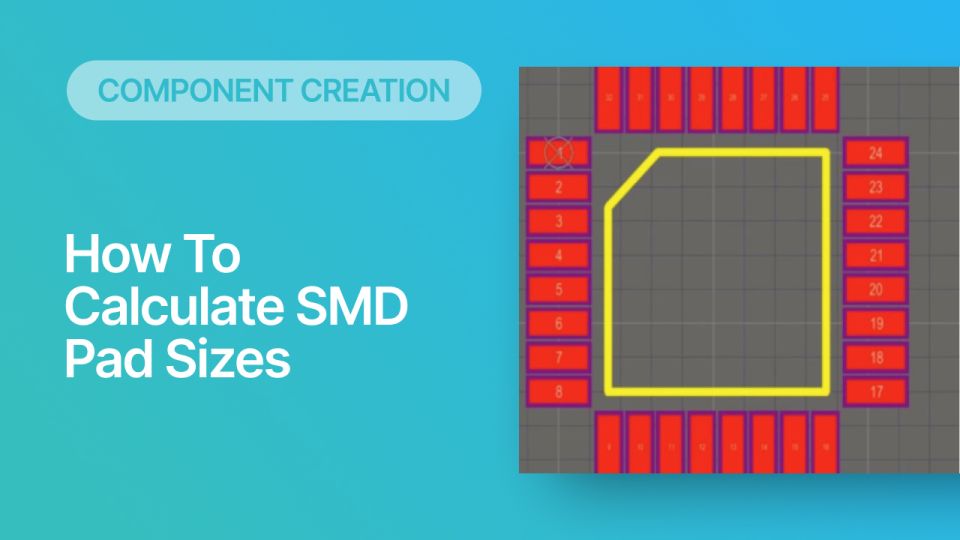
Component creation requires accurate SMD pad sizes in your PCB footprints. See how to determine pad sizes for your SMD components.
A staff member at a PCB manufacturer once explained to me that they thought we were having an issue with
Your BGA fanout strategy depends on the BGA pad size and your pin density. Learn how to pair the right BGA pad size with PCB trace width in this article.
Grounding with an ADC will influence noise injection into the board and it should be dealt with carefully when building a mixed-signal system.
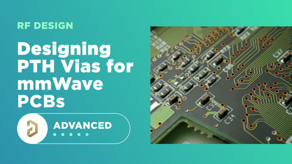
Plated through-hole vias in mmWave PCBs can ruin signal integrity in your RF interconnects if not implemented properly. Learn how to size and place stitching vias in this article.
RF and sensing systems that use MIMO functionality have some important design constraints concerning virtual antenna design and placement. In