Quarter-Wave Transformer Design For Real and Reactive Loads
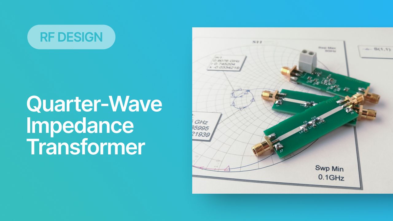
RF systems operate with specific impedance values across entire interconnects, including on PCBs. Not all RF components are packaged in integrated circuits with defined impedances, so impedance matching circuits and line sections are needed to ensure signal transmission between different sections of an interconnect. One of these impedance matching techniques is the quarter-wave impedance transformer, which can be implemented as a printed trace with specific impedance.
An impedance transformer provides a high-Q option for impedance matching right at a target frequency. It is typically implemented as a matching element between a transmission line and a real load. However, it can also be used to match a driver and receiver with real input/output impedances. There is another usage with an additional transmission line section where the quarter-wave transformer can be used to match a load with complex impedance to a real impedance.
How Quarter-Wave Impedance Matching Works
Quarter-wave impedance matching is a technique used in RF PCB design. It is appropriate when an RF signal is operating at a single frequency, or with very small bandwidth (see below for more on this). A quarter-wave transformer is a transmission line with its length equal to one quarter of the wavelength of the signal traveling into a load. This section of transmission line is placed between the feedline matched and a load.
What happens next depends on whether the load is purely real or reactive, as well as whether the driving section is reactive. The quarter-wave impedance transformer technique is generally used in three situations:
- Matching a transmission line to a real load
- Matching a real driver to a real load
- Matching a transmission line to a complex load, but this requires an additional transmission line section
The diagram below shows an example quarter-wave transmission line placed between arbitrary source and load impedances.

The length of the middle transmission lines section is exactly equal to one quarter of the signal's wavelength on the PCB. This means that:
- Quarter wavelength lines only work at the quarter wavelength or odd multiples of the quarter wavelength. They work like high Q bandpass filters with 50 Ohm input impedance.
The function of this section of transmission line is to match the input impedance at the start of the quarter wavelength section to be equal to the driver or feedline impedance. The feedline’s impedance can be anything the designer wants (usually 50 Ohms). Your design goal is to set the quarter-wave section’s impedance (Zq) to take a specific value such that Zin = ZS.
The important thing to note about quarter-wave transformers is that all transmission lines on PCB laminates have reactance in their impedance, but this reactance is small compared to the resistive portion of the transmission line. For example, take a look at the often-quoted dielectric constant of FR4 laminates (𝜀 = 4.4 + 0.02i, and there will be an effective Dk value for microstrips). Transmission lines on real PCB substrates will experience some loss and will therefore always have a small reactive portion of their impedance, but the reactive portion is very small with X/R < 1-2%; this is comparable to the Df/Dk ratio for standard FR4-grade laminates.
If the load impedance is totally real, or if it only has very small reactance, then a quarter-wavelength transmission line on a PCB can be used to directly match the impedance of the load to the feedline or to a driver. This is because the required matching impedance will also be real, and it’s easy to design a transmission line to be very nearly real impedance. However, if the load impedance is complex, an additional section of transmission line would be needed to first transform that load impedance to a real value, and then the quarter-wave transformer is used to match to the target value.
Real (Resistive) Loads
If the load impedance is purely real, then a quarter-wave impedance transformer can be used directly without any additional transmission line sections or components. The diagram below shows how to implement a quarter-wave line for impedance matching between a transmission line and a real load impedance.

The same diagram and procedure can be used to terminate a drive and a load with different real impedances; we simply replace the transmission line Z0 with a driver that has output impedance of Z0. This is a very non-typical case, but it is technically possible with the same procedure shown below.
If we ignore losses momentarily, which is appropriate in short transmission lines and low frequencies, then the input impedance evaluates to:

The final value in the above image is the impedance of the quarter wavelength line to place before the load. You can then use a calculator to determine line width required to hit that impedance value.
The value listed above is not exact, but it is close to being exact. In reality, the target impedance will be slightly reactive because you are taking a hyperbolic tangent of a complex number in the input impedance equation. Therefore, you will end up calculating a complex impedance target that you will never be able to hit perfectly. In the typical treatment of a quarter-wave impedance transformer, this is ignored and the system is considered to be lossless.
Reactive Loads
If the load impedance has a reactive component, then a quarter-wave impedance transformer cannot be used directly. Instead, we would need another transmission line section between the quarter-wave transformer and the load:

Just like the case of a real load impedance, the same procedure applies to a driver by replacing the transmission line Z0 with a driver that has output impedance of Z0.
This problem is more complex because it requires solving for γ1l in the following equation for a chosen value of Z1. An easy solution in terms of transmission line design is to select Z1 = Z0 and determine γ1l from trial and error, or by plotting Im[Zin(1)] on a graph.

In theory, there are infinite numbers of transmission line lengths and widths that will satisfy the above equation because tanh(z) is a periodic function when z is a complex number, which is the general case for any transmission line with losses. The best length value is the shortest length that still hits your width target; this shortest-length line will have the closest resemblance to a lossless line.
Once this length is found, you can use the standard quarter-wavelength impedance match to get the following result:

Don’t forget, in the above equation we have enforced the condition that Z(in)2 = Z0 because we want to match the impedances.
Once the impedance is known, the propagation delay will be known, and then a quarter wavelength for that line can be calculated. This completes the design problem and you now have a quarter wavelength match.
Limitations of Quarter-Wave Impedance Matching
The most important aspect of quarter-wavelength transformer matching is its simplicity because no additional components are needed in the design; everything is printed directly on the PCB. However, the simplicity comes at a cost that should be immediately obvious: these structures only work at multiples of (n + 1/4)λ (n = odd integer), and we generally desire the shortest structure to have minimal loss in the design.
All quarter-wave impedance matching transmission line sections have a couple of drawbacks:
- High-Q matching - As I mentioned above, these structures are like high-Q bandpass filters; they can only provide highly accurate impedance matching at a very narrow range of wavelengths.
- Long lines for reactive impedances - As we saw above, multiple sections are needed to transform the load impedance when the load has some reactance.
- Reactive impedance limits S11 - The lowest S11 value that can be provided by these structures will be limited by the reactive portion of the line and load impedances. If these values were zero, then we would theoretically have S11 = 0 (or -∞).
The first point should illustrate why quarter-wave impedance matching (or any other multiple of wavelength) should only be used for RF signals, and in particular only RF signals with no modulation or very limited modulation: they limit the bandwidth to a very small value that will not be useful for transmitting digital signals. When broader bandwidth is needed, an LC circuit (or a Pi/T filter) should be used to match the impedance, and even then you won’t have perfect matching to some loads.
The second point is not really problematic at high frequencies, but it is a challenge at low frequencies. Consider sub-GHz radios operating at 900 MHz; the quarter wavelength of a microstrip line operating at this frequency on a Dk = 4 substrate would be about 5 cm (assumes Dk effective is about 3). If you then have another line that is cascaded to this to match a reactive load, the total cascaded line length could be anywhere from 5 to 25 cm. This requires a very large board size that may not be practical at low frequencies.
The table below summarizes the performance characteristics of each type of matching noted in this section.
|
|
|
|
|
|
|
|
|
|
|
|
|
|
|
|
|
|
|
|
If you need broader bandwidth impedance matching, then you might consider using a taper to match impedances. Taper matching provides the same function as a quarter wavelength impedance transformer, but certain taper designs can limit S11 below some maximum value over a broader bandwidth than a quarter wavelength line. The example linear taper result below shows a result for a taper targeting an 80 GHz carrier frequency.

I’ll cover the important aspects of taper design in an upcoming article. These taper structures are important in two aspects: for impedance matching between two transmission lines (or with a real load), and for impedance matching across a via transition. The latter is where I have implemented tapers in radar designs where long feedlines need to span across top and bottom surfaces of a board.

