Create high-quality PCB designs with robust layout tools that ensure signal integrity, manufacturability, and compliance with industry standards.
Zach chats with Altium's Vice President Lawrence Romine about the exciting future of PCB Design. Listen to this episode to learn more about Altium's mission.
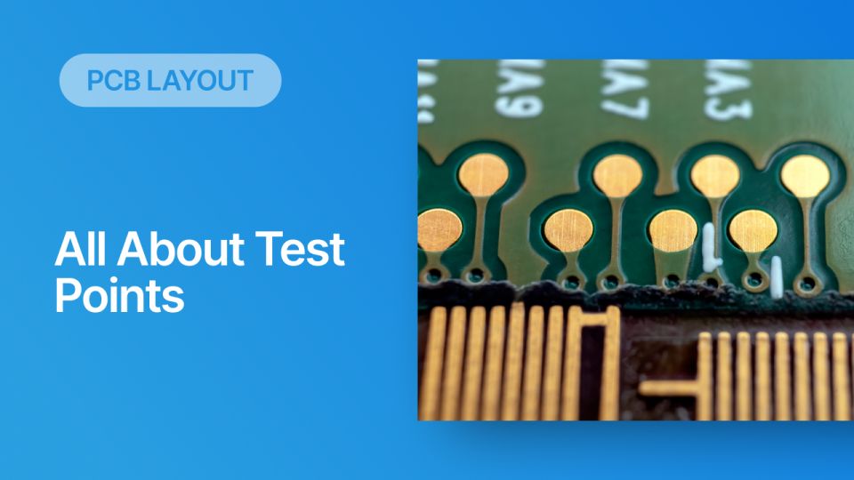
A PCB test point can be a simple pad in the PCB layout, or it can be a specific component where you can connect a probe.
Semi-Additive Process (SAP) is an additional tool in the PCB fabricators' toolbox that supports low-volume, high-mix applications. Read this article to see the detailed process of how SAP works and how it can apply to your next SAP PCB design.
Electrical engineering design reviews should focus on manufacturability, functionality, and reliability. Here’s how to solve your design review challenges.
Your electronics project conception management is essential to identifying risks, establishing the product’s viability, and setting reliable development timescales and budgets. Expert Mark Harris explains the importance of project conception in this article.
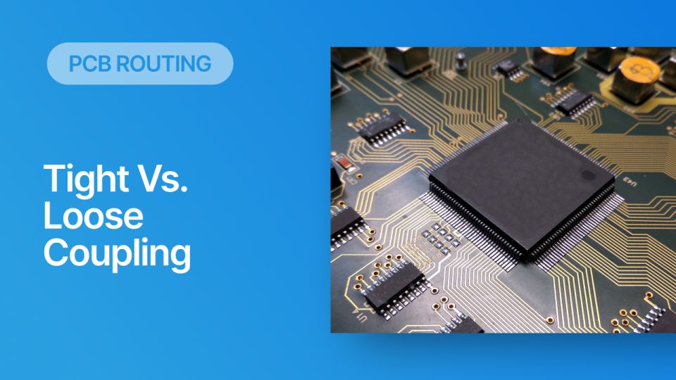
We get a lot of questions about trace impedance and how to calculate the right trace size to hit a
Recently IPC and Altium formally announced that IPC is joining the growing body of the Nexar ecosystem. In this interview