


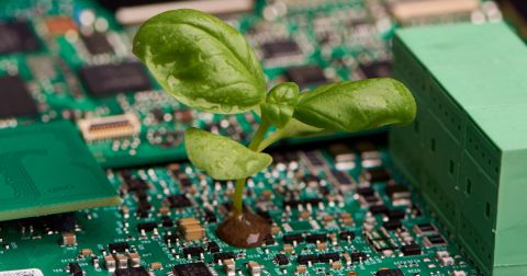


What is the PCB Supply Chain?

At a Glance
The PCB supply chain encompasses all portions of PCB manufacturing processes, reaching from raw materials to components. Learn more about the PCB supply chain in our guide.


The PCB supply chain encompasses multiple components, raw materials, and the PCB itself. PCBs and PCB assemblies (PCAs) are often the most technically complex components that are purchased for electronic assemblies and products, and they form the center of an electronic product's universe. The complexity of modern PCBs leads to several challenges for a supply chain management (SCM) team that may be significantly different when compared with other commodities the team manages.
In this brief guide, we'll look in-depth at the PCB supply chain, and specifically what falls within the purview of a procurement and supply chain management team.
- Anatomy of the PCB Supply Chain
- Who Manages a Product's Supply Chain?
- PCB Supply Chain Management Challenges
- PCB Value Delivery Chain
- Product Qualification
- Summary
Anatomy of the PCB Supply Chain
The supply chain for PCBs and PCBAs encompasses a range of raw materials vendors, manufacturers, and of course, the components that appear on a finished PCB. Each step along the supply chain from design concept to finished product draws resources from multiple areas:
- Bare board core and laminate materials, some of which may have compatible swaps as defined in slash sheets; these draw resources from their own supply chain in terms of chemicals and raw materials.
- Bare board raw materials, namely copper foils and woven fiberglass for constructing laminates.
- Additional raw materials, such as cleaning products and solder for assembly, as well as materials and chemicals used in the PCB manufacturing process.
- Tooling and materials used in production of bare boards and assembly of PCBAs, spanning across solder materials, coatings, plating precursors, cleaning materials, and other consumables.
- Semiconductors and other components that are mounted to the PCB to give the device its functionality. PCBAs require a broad range of components to support the desired functions and capabilities in a given product, which could create risk if not selected with an eye towards sustainability.
- Packaging and enclosure materials, or pre-formed enclosures, which will house the finished assembly and enable connectivity with other systems.
Part of the challenge in managing the PCB supply chain is to ensure new products are manufacturable at the desired scale and over the desired product lifetime. For example, ensuring a long-term sustainable supply chain is less important when producing QTY 1 of a complex system, whereas it could be much more difficult when producing a forecasted quantity of millions over a 10+ year period. This is also an important consideration in product lifecycle management as product lifetimes will end once raw materials and components go EOL.

Who Manages a Product's Supply Chain?
Once a product's requirements are defined and engineering starts to work, it is the design of the PCB and selection of components that will start a Value Chain of Events (see below). The layout of the printed is the first physical representation of that product. Design for manufacturing (DFM) is required as a way of optimizing performance and cost, yet also to ensure a design can be manufactured at the desired scale given a manufacturer's fabrication and assembly capabilities. The challenge of managing the information, documentation, and transfer in order to specify the design requirements and other expectations for the suppliers.
-
Procurement: Unless an OEM is one of the few that is vertically endowed with manufacturing, the general considerations for PCB and PCA sourcing decisions, and the criteria that should be used to evaluate and select suppliers is turned over to purchasing.
-
Supplier selection and qualification: Others are involved in the business considerations and selection criteria described to evaluate and qualify suppliers, including processes to perform technical assessments of samples provided by the supplier.
-
Process control, monitoring, and inspection: An ongoing task in managing the electronics supply chain is the monitoring of quality assurance methodology, often based on best quality practices like six sigma principles, with specific recommendations for process control, testing, and inspection of PCBs and PCAs at the supplier.
-
Product acceptance and feedback: Finally, processes must be in place for design qualification, lot acceptance, and ongoing inspection of received PCBs and PCBAs. It also includes recommendations for long-term supplier management that minimize the internal management cost while maintaining a high level of performance.
PCB Supply Chain Management Challenges
Electronics supply chain management carries several challenges not seen in other industries. This is partially due to the complexity of electronic products and systems, both at the bare board level and at the individual component level. Some examples of electronics supply chain challenges are as follows:
-
PCBs and PCAs are custom-designed and therefore cannot simply be purchased from a catalog. In effect, there are no perfect replacements for boards in a larger assembly or system. In addition, if the board fails, an entire subsystem may effectively fail and an entire PCBA will need to be replaced. There are many suppliers, but their capabilities and performance vary widely, requiring more attention to supplier selection and qualification.
-
Just like bare PCBs, not all semiconductors have perfect or comparable replacements. Sometimes, you have to intentionally under-design a board so that multiple PNs in a product family can be used in the PCBA as this helps overcome semiconductor shortages. Another practice one the design side is to implement multiple variants and manage their lifecycles individually.
-
A wide variety of manufacturing processes are used to create PCBs and PCAs, ranging from precise photoimaging and component placement, mechanical presses for lamination and ovens for solder reflow, wet chemical plating and etching, and high-speed drilling and routing. Each of these requires their own tooling and raw materials that do not have perfect replacements.
-
PCBs and PCAs are required to perform as part of an electrical system, and that performance is critical to the success of the final product. The PCB obviously provides interconnections between components attached to the board, but in some cases, it operates as an component in its own right. It may not be possible to determine whether the PCBA works correctly until your design team has evaluated it as part of the final product.
-
Although components on a prototype PCBA can be replaced, traces cut, and jumpers added, PCBs and PCAs cannot be easily reworked, returned, or recycled if the product requirements change, which can lead to additional cost and unwanted inventory.
This is just a sampling of some challenges that arise in the fast-moving electronics supply chain, specifically around semiconductor sourcing and fabrication. Working with other vendors, logistics, and assembly adds to the complexity of PCBA sourcing and procurement.
PCB Value Delivery Chain
VALUE is defined as “Benefits Minus the Costs”. To have a successful product for a market, in each step of the Supply Chain, each segment must perceive value! As seen below, each segment has the next segment as a customer. Thus, each segment contributes to the value chain.
The choice of a specific supplier depends on the relative importance of several different dimensions of supplier performance (see the table below). Suppliers have inherent capabilities and strengths that are based on their own strategic decisions about how they choose to compete. Those capabilities will determine how well they fit the sourcing strategy and how they are likely to perform as an ongoing business partner. Understanding what is most important to the business will guide initial supplier selection and determine whether the supplier’s performance continues to meet your requirements.
|
|
|
|
|
|
|
|
|
|
|
|
|
|
|
|
|
|
Product Qualification
When a new product is conceived, one of the first activities is to break the product down into components or partitions that will allow it to be designed, manufactured, sold, and supported. However, qualification standards may be in order, depending on the target market and industry. This is extremely important since a mistake here may result in a product without the right features, a product that may cost too much, or one that may not meet the required performance standards.
PCB Design and PCB Layout
Many challenges must be faced when designing a new board. The wiring models are important to know in order to select proper design rules and constructions. With blind and buried vias, the new structures are more varied and complicated than conventional boards. Knowing what is cost-effective from a design-for-manufacturing perspective is essential.
Special design rules must be considered with complex structures. Each manufacturing process may have special considerations and limits. Design tools, pad stacks, and auto-routers are all used differently in complex designs. The customization of the design process is not an activity yet. The newer CAD systems also have expert systems available that provide much-needed advice. Manufacturability Audit software concludes the layout process with a thorough check for any mistakes or errors.
PCB Fabrication and Testing
Of the entire value delivery chain, fabrication has become the most established. Currently, over two hundred companies worldwide are using at least twenty different processes to make essentially the same HDI/SLP structures. For example, making the microvia is the easy part, since lasers, etchers and photo-dielectrics have been rapidly improving over the years. The challenges are the basics: registration, fine line lithography, metallization and plating. On complex HDI/SLP, all of these must perform at a superior level. While this is certainly taxing, it benefits all printed wiring board manufacturing processes.

PCBA Qualification and Testing
Assembly has a new value to deliver with complex-fine-pitch components. Components can be closer together, which can change reflow profiles and repair. As the topside fills up, the opposite side also must take more components including many ones. This also will alter the assembly process and reflow profiles. With newer smaller and denser area array components like chip scale packages or flips chip, the total number of connections per square centimeter increases dramatically. These newer smaller components with underfill or very high surface connection densities may have a reliability interaction with complex structures. Thin structures are more likely to flex during thermal cycles and this introduces new mechanisms and opportunities for failure, which must be thoroughly evaluated and tested.
The final stage of the PCB value chain is assembly level testing. This presents very new issues with the new smaller area array components. If via-in-pads are used with the area array components, after assembly there are no breakout vias to use to test probes. Design-for-Test becomes a major ingredient for system partitioning. Testing from the perimeter, boundary scan or built-in-self-test becomes a major design factor. Components may be so close now that test pads are either too large or there is no room to get a test pin into the area. Adding test pads to the surface after the board is designed can severely add to its complexity and cost, as well as add detrimental parasitics. Newer assembly level verification schemes will probably be developed that do not require the classical bed of nails fixtures, replacing them with faster non-contact test techniques.

Summary
In all, PCB supply chain developments arise quickly and will create multiple challenges for design and manufacturing teams. The last thing anyone wants to hear is that a product can't be produced at scale because a single resistor can't be procured. Working together and realizing that each part of the delivery will depend on the other links of the chain, we can provide solutions to the OEM allowing them to deliver superior products.
When you need an instant look into the PCB supply chain as you select components and plan or fabrication, use the complete set of CAD tools in Altium Designer®. Once your design is ready for a thorough design review and manufacturing, your team can share and collaborate in real time through the Altium 365™ platform. Design teams can use Altium 365 to share manufacturing data and test results, and design changes can be shared through a secure cloud platform and in Altium Designer.
We have only scratched the surface of what’s possible with Altium Designer on Altium 365. Start your free trial of Altium Designer + Altium 365 today.

About Author
Related Resources
Related Technical Documentation
Table of Contents
Design to Release, Without the Friction
- Keep reviews tied to the right version
- Reduce handoff confusion and rework
- Spot sourcing and release risk earlier
- Work solo, share when needed
Get Started
Thank you, you are now subscribed to updates.

